In the design process of high-speed PCB, wiring is the finest and most qualified, and engineers often face various problems in this process. This article will first introduce the basics of the PCB, and at the same time make a brief explanation of the wiring principle, and finally bring the very practical four PCB wiring skills and essentials.
Here are some good wiring tips and tricks:
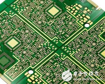
First of all, let's start with a basic introduction. The number of layers of PCB can be divided into single layer, double layer and multi-layer. The single layer is now basically eliminated. The double-layer board is used in a lot of sound systems. Generally, it is used as a rough-type board for power amplifiers. Multi-layer boards refer to boards of 4 layers and 4 layers or more. Generally speaking, the density of components is not high. Will suffice. From the perspective of the via, it can be divided into through holes, blind holes, and buried holes. A through hole is a hole that passes directly from the top layer to the bottom layer; a blind hole passes through the hole from the top or bottom layer to the middle layer, and then does not continue to be worn. This advantage is that the position of the via hole is not blocked from the head to the tail. The other layers can still be routed at the location of the via; the buried via is the via from the middle layer to the middle layer, buried, and the surface is completely invisible. The details are shown in the figure below.
Before the automatic wiring, the wires with higher requirements are pre-wired in advance, and the edges of the input end and the output end should not be adjacent to each other to avoid reflection interference. If necessary, the ground wire can be isolated for isolation, and the wiring of two adjacent layers should be perpendicular to each other, because parallelism is more likely to cause parasitic coupling. The routing rate of the automatic wiring depends on a good layout, and the wiring rules can be set in advance, such as the number of wire bending times, the number of via holes, the number of steps, and the like. Generally, the exploration wiring is first performed, the short wires are quickly connected, and the routing of the wires to be routed is optimized by the labyrinth wiring. It can disconnect the laid wires and try to re-route as needed to improve. Overall wiring effect.
For layout, one principle is to separate the numbers and simulations as much as possible, so that one principle is that low speeds should not be close to high speed. The most basic principle is to separate the digital ground from the analog ground. Because the digital grounding is a switching device, the current is very large at the moment of the switch, and it is small when it is not moving, so the digital grounding cannot be mixed with the analog ground. A recommended layout can look like the image below.

(1) Add a decoupling capacitor between the power supply and ground. Be sure to connect the power supply to the pin of the chip after the decoupling capacitor. The following figure shows several wrong connection methods and a correct connection method. Do you make such mistakes against the reference? Decoupling capacitors generally have two functions, one is to provide the chip with a large current, and the other is to remove the power supply noise. On the one hand, the noise of the power supply is minimized, and the noise generated by the chip is not affected. power supply.

(2) Try to widen the power supply and ground wire. It is better to ground the ground wire than the power cable. The relationship is: ground wire "power cable" signal cable.
(3) A large-area copper layer can be used as a ground wire, and the unused areas on the printed board are connected to the ground, used as a ground wire, or made into a multi-layer board, and the power supply and the ground line each occupy one. Floor.
2. Processing when mixing digital circuits and analog circuits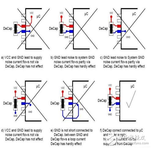
Nowadays, many PCBs are no longer single-function circuits, but are composed of a mixture of digital circuits and analog circuits. Therefore, it is necessary to consider the interference between them when wiring, especially the noise interference on the ground.
Due to the high frequency of the digital circuit, the sensitivity of the analog circuit is strong. For the signal line, the high-frequency signal line should be as far away as possible from the sensitive analog circuit device, but for the entire PCB, the ground line of the PCB is connected to the outside node. There can only be one, so it is necessary to deal with the problem of digital circuit and analog circuit common in the PCB. In the circuit board, the ground of the digital circuit and the ground of the analog circuit are actually separated, but the PCB is connected to the outside world. Interface (such as plugs, etc.). The ground of the digital circuit is short-circuited with the analog circuit. Please note that there is only one connection point and there is no common ground on the PCB, which is determined by the system design.
3, for the treatment of line cornersUsually there will be thickness changes at the corners of the line, but some reflections will occur when the line diameter changes. The corner method is the worst for the thickness of the line. The right angle is the worst, the 45 degree angle is better, and the round corner is the best. However, rounding is more troublesome for PCB design, so it is generally determined by the sensitivity of the signal. The general signal can be used at a 45-degree angle. Only those very sensitive lines need to be rounded.

No matter what you do, check it after you finish it. Just like when we have the time to check, we have to check our answer. This is an important way for us to get high scores. The same is true for us to draw PCB boards. In this way, we can be more confident that the circuit board we draw is a qualified product. We generally check the following aspects:
(1) Line and line, line and component pad, wire and through hole, component pad and through hole, whether the distance between the through hole and the through hole is reasonable, and whether the production requirements are met.
(2) Whether the width of the power line and the ground line is appropriate, whether the power supply and the ground line are tightly coupled (low wave impedance), and whether there is a place in the PCB where the ground line can be widened.
(3) Whether the best measures are taken for the key signal lines, such as the shortest length, the protection line, the input line and the output line are clearly separated.
(4) Whether the analog circuit and the digital circuit part have separate ground lines.
(5) Whether the pattern (such as illustration and labeling) added to the PCB will cause a signal short circuit.
(6) Modify some unsatisfactory lines.
(7) Whether there is a process line on the PCB, whether the solder mask meets the requirements of the production process, whether the solder mask size is appropriate, and whether the character mark is pressed on the device pad, so as not to affect the quality of the electrical equipment.
(8) Whether the edge of the outer frame of the power supply layer in the multilayer board is reduced, for example, the copper foil of the power supply ground layer is likely to cause a short circuit outside the exposed plate.
In short, the above tips and methods are all about experience. It is very worthwhile for us to learn from the PCB board. In addition to the skillful use of the drawing tool software, we must have solid theoretical knowledge and rich practical combat. Experience, these can help you complete your PCB diagram quickly and efficiently. But it's also very important, that is, be careful, whether it is wiring or the overall layout, every step must be taken very carefully, because a small mistake you may cause your final product to become a waste, and then look for Nothing goes wrong, so we would rather spend more time checking the details and not willing to go through the process of drawing, so it might take more time. In short, the process of drawing a PCB pays attention to the details.
——Part of the reference content source "One of the high-speed PCB design guidelines"
FRP Drainage Channel,frp trench drain,Trench Drain System,Grating Trench Cover
Hebei Dingshengda Composite Material Co., Ltd. , https://www.dsdfrp.com