Abstract: Software radio technology is increasingly used in various fields of modern communications. This article introduces a common satellite measurement and control platform based on high-speed DSP chips. The working parameters of the universal platform such as modulation mode, code rate, carrier frequency, command data format, and modulation code type are fully programmable.
Software radio is developed with the rapid development of computer technology and high-speed digital processing technology. The basic idea is to bring the broadband A / D / A converter as close to the antenna as possible, and to try to keep the various functions of the radio in an open , Modular platform is determined and implemented by software. The system operating parameters such as modulation mode, code rate, carrier frequency, command data format, and modulation code type of the platform are fully programmable.
The traditional satellite measurement and control platform has the problems of imperfect performance, inflexible configuration of modulation mode, subcarrier, and code rate, and large volume. Develop and develop a universal, integrated, and intelligent measurement and control platform. By injecting different software, the modulation carrier frequency, modulation mode, transmission code rate and other parameters can be changed. It is used in telemetry and remote control tasks for various orbit satellite platforms. The digital signal processor (DSP) is the soul and core of the entire software radio solution. The characteristics of flexibility, wife opening and versatility of the universal platform are mainly realized by the universal hardware platform and DSP software centered on the digital signal processor. After comparison, we use TI's TMS320C6000 series DSP chips and matching peripheral chips to form a set of real-time DSP systems.
Figure 1 TMS320C6701 block diagram
1 DSP technology of software radio general platform
1.1 Introduction of TMS320C6701 DSP chip
TMS320C6701 is TI's high-performance DSP chip, with a structural block diagram shown in Figure 1.
The main features of TMS320C6701 are:
* Single instruction word length is 32 bits, 8 instructions form an instruction packet, the total word length is 256 bits, the pin is compatible with the pins of TMS320C6201 series.
* The system structure adopts very long instruction word (VLIW) structure; 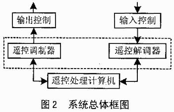
* The hardware supports IEEE standard single-precision and double-precision instruction sets, supports byte addressing to obtain 8-bit / 16-bit / 32-bit data, and there are bit manipulation instructions in the instruction set (including bit field extraction, setting, clearing, and bit count and return) One, etc.);
* 1Mb (bit) of on-chip storage space, of which 512Kb for program storage space and data storage space;
* 32b External Memory Interface (EMIF), 52MB external memory addressing capability;
* Four-channel self-loading DMA coprocessor, which can be used for DMA transmission of data;
* 16-bit host interface (HPI);
* Two multi-channel buffered serial ports (McBSPs);
* Two 32-bit general-purpose timers;
* Flexible phase-locked loop (PLL) clock generator, which can perform different frequency multiplication processing on the input clock;
* There is IEEE1149.1 standard boundary scan emulator (JTAG) inside the chip, which can be used for chip self-test and development;
* A total of 352 feet of the chip are packaged in BGA to obtain good high-frequency electrical performance and make the chip size smaller;
* Adopt 0.18μm technology, then five layers of metal, input and output interface voltage is 3.3V, core voltage 1.8V (1.9V at 167MHz).
1.2 Application of DSP technology in software platform
Each set of measurement and control platform contains dual-mode backup remote control modulator and remote control demodulator, and the two sets are powered by independent power sources. The overall block diagram of the system is shown in Figure 2. The modulator and demodulator communicate with the remote control processing computer through different RS232 serial ports, respectively, to complete the control of the modem and the sending and receiving of data. 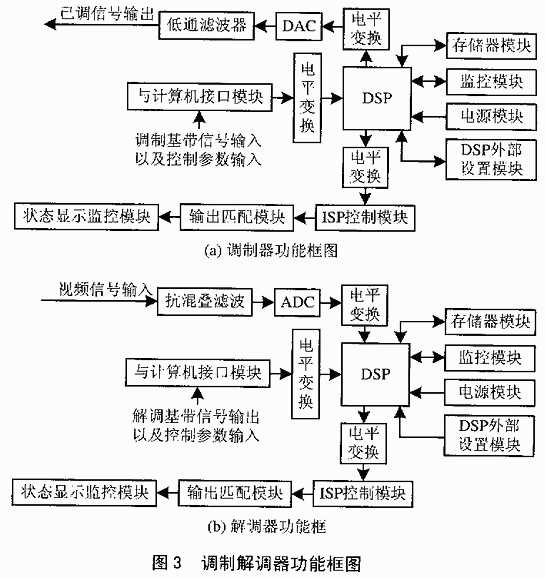
Before each task, the user sets the modulation mode, modulation parameters and communication connection mode through the control computer, and calls the algorithm parameter generation program to generate the preset parameters of the algorithm in the modulator and demodulator, and from the batch data when the device is initialized. The serial port is sent to the DSP chip and sent to the Flash ROM after verification. In order to ensure the reliability of program transmission, IRQ error control mode is adopted. Each time a data packet is received by the DSP, the data information is returned to the computer while it is stored. Once the computer finds a data error, it transfers to the retransmission mode. After the parameter setting is successful, the modem sends and receives remote control commands according to the protocol, and returns the working status to the remote control processing computer, which is also displayed on the front panel of the remote control.
1.3 Modulator and demodulator hardware structure and function description
The hardware system uses DSP as the core, and the peripheral circuit is mainly composed of the following modules: power module, system clock and mode setting module, memory module, system monitoring module, communication with the control computer module, modulation output module, B code clock receiving module and display Control module. In the demodulation system, except for the demodulation input module, decryption interface module and display control module, the remaining modules are consistent with the modulation system, as shown in Figure 3. 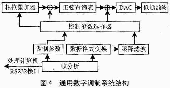
When the modulator is powered on, the DSP first completes self-loading through the external memory module. After the self-loading is completed, the DSP main program initializes the parameters of the status display monitoring module. When there is a modulation task, the control computer first sets the DSP parameters (such as filter parameters, modulation system, modulation sub-carrier frequency, modulation code rate, etc.), and then sends the modulation data to the DSP, which is received by the DSP's serial communication port For data, the sub-carrier frequency modulation is completed in the DSP; the modulated data is sent to the digital module through the DSP serial port for digital-to-analog conversion, and the converted signal is output after being filtered by a low-pass programmable filter. The working process of the demodulator is similar to the above. When it is detected that the modulated sub-carrier enters the A / D channel, the demodulation module is started to demodulate, and the demodulated data is sent to the control computer.
2 DSP realizes signal modulation and demodulation
2.1 Signal modulation
The design goal of the modulator is to realize a multi-mode general-purpose modulator with different carrier frequencies, modulation methods, transmission rates and code types on a programmable hardware platform by injecting different algorithms or executing software. It will support the different needs of various communication transmitters with flexible reconfiguration, and is more conducive to the interconnection of various communication devices. Considering that digital direct synthesis technology has the advantages of flexible numerical control, high frequency resolution, fast frequency switching, continuous linear change of phase, large coverage bandwidth, and good orthogonality of the generated sine / cosine signals, our design solution is based on DSPs. As the core, the software DDS technology is used to realize a high-precision, high-performance digital modulator. The overall block diagram of the modulator is shown in Figure 4.
Frame analysis completes the reception, verification and forwarding of program data (send to Flash ROM) when the device is initialized. During normal operation, the modulation parameters and equal modulation data are separated from the frame data and sent to the parameter register and data register respectively.
Figure 5 BPSK receiving overall block diagram
In the data format conversion, complete the conversion of the input data into modulation parameter control words (such as frequency control word K, phase control word φ and sub-degree control word A in the corresponding modulation mode) and the modulated data in the corresponding format. After roll-off processing (no roll-off processing is required for FSK mode), the sinusoidal carrier is modulated.
2.2 Signal demodulation
For BPSK reception, we use coherent demodulation, as shown in Figure 5. After receiving the original signal sequence by band-pass sampling, the received signal is first mixed with the locally generated sine sequence, and then the high-frequency component is removed by low-pass filtering to obtain its signal sample sequence (the frequency and phase of the sine sequence are also Sample sequence obtained). Then, the waveform of the best decision point is estimated on the sample sequence of the baseband signal, and the estimated value is sent to the equalizer for equalization processing, and the equalization structure makes the final demodulation data by making 0 and 1 decisions. The key to demodulation is the synchronization of the local carrier and the extraction of symbol timing errors.
The demodulation method of ASK (FSK) signal can be divided into two types: coherent demodulation and non-coherent demodulation. Due to the strong anti-interference ability of coherent demodulation, this scheme uses coherent demodulation. Figure 6 is a block diagram of the overall demodulation scheme at the receiving end when coherent demodulation is used.
The received signal first passes through a low-pass filter to filter out-of-band noise (the low-pass filter here is designed by a dedicated device). Then, after A / D conversion, the sample sequence is obtained, and according to different stages of the work, it is demodulated in two channels with corresponding local coherent carriers, mainly including two processes of mixing and low-pass filtering. After the demodulated signal passes through the low-pass filter, the baseband signal is recovered. The baseband signal performs bit timing and symbol decision to obtain the final demodulated data.
Figure 6 ASK / FSK coherent demodulation overall process block diagram
3 Conclusion
The software radio universal measurement and control platform is the development direction of the satellite measurement and control platform, which can solve the problems of high development cost, long cycle and poor versatility of the original platform. Taking the new generation DSP chip TMS320C6000 as the core of the software radio platform, it can meet the needs very well, and has greater redundancy, so it can be upgraded.
The small appearance and size of the One Hand Gaming Keyboard is one of the key points for users to choose.The maximum length of the keyboard in one-handed games is usually only half or even less than one third of the standard keyboard.The most comfortable position for both hands is usually slightly larger than the shoulder width of the player (the distance between the tail fingers of both hands is about 500-650mm).When using the standard keyboard, between the mouse and the keyboard. The clearance for Gaming Mouse movement is usually no more than 100mm(standard 104-key keyboard length is about 450mm). And the use of one-handed game keyboard, can let the player play with a wide mouse movement space, so that players enjoy a more rapid and flexible mouse operation.
Due to the limited size of one-handed gaming keyboards, the number of surface keys usually does not exceed the number of keys in the main key area of a standard keyboard (61 keys). Although the current PC games are designed with the first left hand key area, some secondary keys are still designed in the right hand key area for the convenience of players' memory and game operation.
For the one-handed game keyboard, comfortable ergonomic design, is to allow players to maintain long-term combat effectiveness of the basic guarantee. However, it is different from the ergonomic design of mouse in that players often move their fingers up and down and left and right when using the Gaming Keyboard.The ergonomic design that is too close to the palm will lead to the restriction of finger movement. Therefore, the ergonomic design of the one-handed game keyboard must be carried out in order to ensure that the player's finger operation is not affected.

One Hand Gaming Keyboard,Computer Gaming Keyboard,Wireless One Handed Keyboard,Single Hand Gaming Keyboard
Henan Yijiao Trading Co., Ltd , https://www.yjusbcable.com