Description: In this test, four read and write accesses are initiated, in which the read and write operations are separated, and the addresses accessed by four read and write operations are the same, thereby observing the bandwidth overhead introduced by read and write switching. As can be seen from the figure, after performing a read/write operation, even if the address of the next write/read operation does not change, the next command cannot be executed immediately, and it must wait for a while. After measurement, it is found that in the continuous read and write switching process, the total time required for a set of read and write operations is 8000ps+23508ps+8000ps+40492ps=80ns, of which the effective time is 16ns and the bandwidth utilization is 20%.
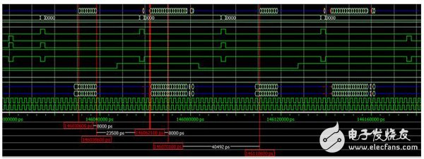
Figure 6 Same bank read and write switching sequence diagram
Six. The same bank different line read and write switching testDescription: In this test, four read and write accesses are initiated, in which the read and write operations are separated, and the addresses accessed by the four read and write operations are in different rows of the same bank, thereby observing the bandwidth overhead introduced by the read and write switches. It can be seen from the figure that due to the read and write switching and row switching, the total time required for a set of read and write operations is 8000ps+35508ps+8000ps+76492ps=128ns, and the effective time is 16ns. It is 12.5%.
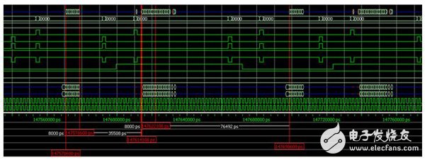
Figure 7 Same line bank read and write switching timing diagram
ConclusionAfter verification of several test items above, it can be found that Xilinx's DDR3 controller combined with DDR3 chip for continuous storage by address, the efficiency is still relatively high, basically can reach more than 95% (some scattered overhead is not calculated in detail, so take 5 % as the sum of these expenses). However, Xilinx's DDR3 controller has a low efficiency for random address access to DDR3. For some table lookup applications, DDR3 access efficiency is very low due to the randomness of the lookup table address.
The reasons for the low random access efficiency are: 1. Switching with Bank line; 2. The number of banks opened at the same time can only be 4; 3. Read and write switching.
The random access DDR3 bandwidth utilization is basically maintained between 11.8% and 40%.
Eight. Solution1. Change the number of banks that can be opened simultaneously to Xilinx's DDR3 controller to 8;
2. Adjust the order of DDR3 access (read or write) to avoid switching with Bank line and read and write switching.
Data Center Power Distribution Monitoring System
Data Center Power Distribution Monitoring System is a multi-circuit measuring system by modular design. It measures 60 circuits for the incomer and feeder cabinet. Connected with the high accuracy hall sensor, the BCM201 Dc Data Center Power Monitoring System provides 0.2S Class measuring parameters such as fundamental parameters and harmonic data. A color 7" HIM with Ethernet interface makes the user easy to over view and control the system in real time.
Data Center Power Distribution Monitoring System,Data Center Dc Power Distribution System,Data Center Power Measuring System,Dc Data Center Power Monitoring System
Jiangsu Sfere Electric Co., Ltd , https://www.elecnova-global.com