You have to make some design trade-offs when doing more complex board designs. Because of these trade-offs, there are factors that affect the design of the power distribution network of the PCB.
When the capacitor is mounted on the PCB, there is an additional loop inductance that is related to the mounting of the capacitor. The magnitude of the loop inductance value is design dependent. The size of the loop inductance depends on the line width and line length of the line from the capacitor to the via. The length of the trace is the connection capacitance and the power/ground plane length, the distance between the two holes, the diameter of the hole, and the pad of the capacitor. ,and many more. Figure 1 shows the mounting patterns for various capacitors.
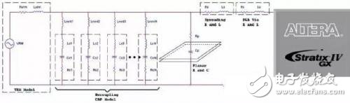
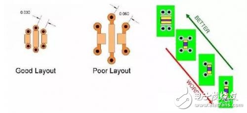
Figure 1 Best and worst capacitor layout
Design points to reduce the inductance of the capacitor loop:
â– Place the hole as close as possible to the capacitor. Reduce the hole spacing of the power supply/ground. If possible, use multiple pairs of power/ground holes in parallel. The two holes, such as the opposite polarity of the current, are placed as close as possible, and the holes of the same polarity are placed as far as possible.
â– Use short and wide traces to connect the holes and capacitor pins.
â– Place the capacitors on the surface of the PCB (top and bottom) as close as possible to their respective power/ground planes. This can reduce the distance between the holes. Use a thin electrolyte between the power supply/ground.
The next is the design of three different cases for the installation and propagation of the capacitor. Figure 2 shows the introduction of loop inductance for various design scenarios.
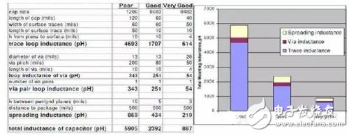
Figure 2 Design situation

15v wall charger,15 Watt Power Supply,15v ac dc adapter,AC Wall Charger Power Adapter,AC/DC Charger Power Supply Switching Adapter,DC 15V Global AC / DC Adapter,15VDC Power Supply Cord Cable Wall Charger,15VDC800 Charger PSU
Shenzhen Waweis Technology Co., Ltd. , https://www.laptopsasdapter.com