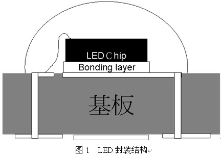
Figure 1 shows the structure used in the current high-power LED package. The LED chip is first packaged on the heat-conducting substrate, and then the gold wire and the sealant are used. The LED package structure has the advantages of light weight, high thermal conductivity and simple circuit, and can be applied outdoors. And indoor lighting. Among the choice of substrate, alumina (Al2O3) and silicon (Si) are materials that have been applied in the market at present. Among them, the alumina substrate is an insulator and must have a conduction heat design, and the copper layer is thickened by electroplating to 75um; Silicon is an excellent thermal conductor, but it has poor insulation and must be insulated on the surface.
Alumina substrates and silicon substrates have been used in high-power LED packaging. Since LED luminous efficiency still needs to be improved, heat is still an important problem that must be solved when using LED lamps. Therefore, LED thermal conduction functions must be carefully analyzed. To analyze the thermal conductivity function, the thermal resistance meter must be used for measurement. The following analysis will subdivide the LED package structure, including the chip layer, the bonding layer and the substrate layer, to analyze the thermal resistance of each layer. The analysis tool is the most recognized in the world. T3Ster instrument.
This article will briefly analyze the performance of the thermal resistance of the alumina substrate and the silicon-based LED board package (T3Ster instrument measured), the proper nouns are defined as follows:
Rth: thermal resistance, the unit is (oC/W), the formula is T / KA;
T: thickness of the thermally conductive substrate (um);
K: thermal conductivity of the thermally conductive substrate (W/mC);
A: Heat transfer area (mm x mm).
The application of alumina in LED packaging is mainly due to the high insulation of alumina materials and the fabrication of light components. However, the application of alumina substrates in electronic components is caused by the low thermal conductivity of alumina materials (about 20K/W). High thermal resistance. Figure 2 shows the results of the T3Ster thermal resistance tester E company's alumina substrate package LED (LED area: 1 x 1 mm; LED emitter: 3.15x3.5 mm). When tested at 25 °C ambient temperature, each package layer The thermal resistance is as follows:
1. Chip: 2 oC/W
2. Bonding layer : 3 oC/W
3. Alumina substrate: 20 oC/W (high thermal resistance, poor substrate fabrication)

When a small current of 175mA is applied to the 1 x 1 mm2 LED chip, the temperature rise of the alumina substrate due to the thermal resistance is 10.5oC (=20x175mAx3.0V), heat is not easily conducted out of the LED chip; when 350mA current is passed in 1 x On a 1 mm2 LED chip, the temperature rise of the alumina substrate due to thermal resistance is 23oC (=20 x 350mAx3.3 V), at which time the alumina substrate will not be able to conduct heat out of the LED chip, and the LED chip will generate a lot of light decay; When a large current of 500 mA is applied to a 1 x 1 mm2 LED chip, the temperature rise of the alumina substrate due to thermal resistance is approximately 36 oC (20 x (500 Ax3.6 V), at which time the alumina substrate will not be able to When the heat is conducted out of the LED chip, the LED chip will quickly decay. Therefore, if the aluminum substrate is selected for the LED chip package, the package component is only suitable for low power (~ 175 mA, about 0.5 W) because of its high thermal resistance.