1 Introduction
This article refers to the address: http://
With the rapid development of China's national economy, the construction of domestic highways, urban roads and parking lots is increasing, and the requirements for traffic control and safety management are also increasing. Intelligent Transportation Systems (ITS) has become the current The main direction of traffic management development, and License Plate Recognition (LPR) system technology plays an important role as the core of intelligent transportation system. It is indispensable in project management such as highways, urban roads and parking lots. The important position of substitution [1-2].
The license plate recognition system studied in this paper is proposed in this context. For the current LPR as the core key technology in ITS, it has considerable theoretical and practical significance. The system is designed with an embedded license plate recognition system based on DSP and FPGA [3-4]. This system is different from the traditional license plate recognition system. The specific implementation process will be described in detail below.
2, system structure design
The traditional license plate recognition system is mainly realized by the method of constructing several main modules of camera, video capture card and industrial computer. The advantage is that it is easy to implement, but the cost is high, the real-time performance is not strong, and the installation and maintenance are inconvenient. In the system design of this paper, the traditional mode is abandoned. TI's TMS320C6713B high-performance (powerful parallel computing capability) DSP is used as the operating hardware platform for the recognition algorithm. Altera's cost-effective Cyclone series EP1C12Q240 model FPGA is used as the coordination. The whole system work and related image acquisition and control, together with some peripheral devices (FLASH, SDRAM, etc.) together constitute the hardware platform of the embedded license plate recognition system, as shown in Figure 1.
Different from the traditional license plate recognition system, the system can realize the collection, recognition and output of license plate images without a computer. It has the characteristics of high recognition performance, strong environmental adaptability, simple installation and maintenance, and low cost. The system design with DSP and FPGA as the core has the advantages of flexible structure, versatility and modular design, so that high-efficiency algorithms and real-time control can be realized. At the same time, the development process can be carried out in parallel.
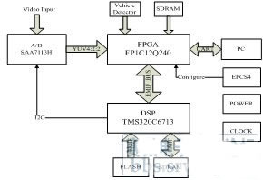
Figure 1 license plate recognition hardware block diagram
2.1 video input module
At present, there are three kinds of TV signal systems in the world, such as NTSC system, PAL system and SECAM system. Most countries in the world adopt PAL system, and China also adopts PAL system. The video signal output by the camera used in this system is standard. PAL system.
The PAL TV system stipulates that the field scanning frequency is 50 Hz, and 25 frames of images are scanned every second. Each frame includes odd and even two fields of images, and the number of scanning lines per frame is 625 lines. The television signal consists of an "image signal" and a "composite synchronization signal" that ensures synchronization and an auxiliary signal such as a "composite blanking signal" that eliminates the scanning of the flyback retrace line. After the PAL TV signal is converted into a digital video signal, the general output data format conforms to the ITU656 YUV 4:2:2 standard, and 625 lines of data of one frame of image are output, wherein the effective image data occupies 572 lines, and the other is a field blanking signal; The effective image data per line is only 720 pixels.
The input in this system is the analog image data of the PAL system, which must be A/D converted for subsequent system processing. The video decoding chip (A/D) selected by this system is the SAA7113H [5] of Philips, which supports standard PAL video signal input. The input can be 4 CVBS or 2 S-video (Y/C) signals. The input can be converted by different configurations of internal registers, and the 8-bit "VPO" bus and some field and line synchronization control signals are output, and the image data is output. Standard ITU656 YUV4:2:2 format. The SAA7113H has a series of registers inside, which can be configured as different parameters. The control of chromaticity, brightness, etc. is performed by rewriting different values ​​to the corresponding registers. The reading and writing of the registers needs to be performed through the I2C bus. Because the TMS320C6713 has its own I2C bus interface, the system design uses the DSP to control the SAA7113H through the I2C bus, which makes the system design easier [6].
The VPO[7:0] bus of the SAA7113H and the RTS0, RTS1, and LLCLK are connected to the FPGA, and the RTS1 and RTS0 of the SAA7113H are respectively configured as field and line synchronization signals through the I2C bus of the DSP, and only when the line sync signals are simultaneously active, It is the effective image data output, otherwise it is generally the image blanking signal. At this point, we only need to collect the data on the VPO bus according to the LLC clock to get the complete image data (720 * 572 size). The connection between the SAA7113H and the DSP and FPGA is shown in Figure 2.
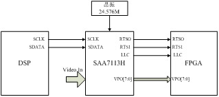
Figure 2 Schematic diagram of the connection between SAA7113H and DSP and FPGA
After the actual operation, it is correctly configured by the DSP's I2C bus, and then the FPGA program written by Verilog is used to sample the image data, and then the waveform is correspondingly calculated by the Quartus II's own SignalTap II Logic Analyzer. Analysis and verification of some important signals in the system, the results show that it is correct and feasible. Figure 3 shows the relationship between the line and field sync signals RTS0, RTS1 and the VPO data output, and the expected result is achieved.
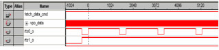
Figure 3 Line sync signal (RTS0, RTS1) and VPO waveform
2.2 DSP function module
As the core chip of this system, DSP has two key technologies: one is the construction of DSP hardware platform; the other is the development of DSP program, including DSP algorithm migration and low-level driver writing.
2.2.1 DSP hardware construction
The TMS320C6713B is a high performance 32-bit floating point DSP from TI [7]. It operates at up to 300MHz and can execute 2400MIPS and 1800MFLOPS per second, making it ideal for use in large data processing applications. It integrates a wealth of on-chip peripherals, including PLL, multi-channel EDMA controller, multi-channel buffer serial port (MCBSP), I2C interface, HPI interface, EMIF interface. The 32-bit high-performance external memory interface (EMIF) can be easily and seamlessly interfaced with synchronous/asynchronous memories such as SRAM, SDRAM, SBSRAM, and is compatible with the 8/16/32-bit external memory bus [7]. The FLASH, SDRAM and FPGA on the system are hung on the EMIF bus of the DSP to facilitate the access and operation of the DSP:
(1) DSP and FLASH interface: FLASH is a high-density, non-volatile electrical rewritable memory, mainly used to store some applications and other information to ensure that power is lost without losing data. The FLASH chip used in this system is SST's SST39LF1601, which has a capacity of 2 Mbytes and can operate at 3V~3.6V with an access speed of 70ns. And the FLASH is mapped on the CE1 space of the DSP, and the corresponding mapping address is 0x90000000-0x901FFFFF. The advantage of mapping to the CE1 space is to facilitate the BOOTLOADER of the program. After the DSP power-on reset, the internal EDMA controller of the DSP will copy the 1KB data of the CE1 space to the internal memory at the address 0 by default, and then run. So as long as the application is programmed into FLASH, the system can run off the computer. Another role of FLASH here is to save some character template information, feature point information and some user information for the license plate processing algorithm.
(2) DSP and SDRAM interface: SDRAM is an abbreviation of Synchronous Dynamic RAM. Its main features are: synchronous access, read and write operations require a clock; second, dynamic storage, the chip needs to be refreshed periodically. . The internal storage capacity of the TMS320C6713 cannot meet the needs of the system program, and the expansion of the high-speed memory is required to provide the running space of the system program. In this system, a 16-bit SDRAM HY57V641620 from Hydix is ​​used, which has a capacity of 8M. It is used for data temporary storage of the DSP when processing the license plate, and maps it to the CE0 space of the DSP. The corresponding address is: 0x80000000 -0x807FFFFF. Its working clock is provided by DSP, and the system is set to 100MHz. Various parameters of the SDRAM can be set by configuring the EMIF control register of the DSP.
(3) Connection between DSP and FPGA: The FPGA captures the license plate image from the video stream. How to let the DSP acquire the image information for processing is also a key point of the system design. SBSRAM (Synchronous Burst Static RAM), the synchronous burst static memory, has the greatest advantage of supporting synchronous burst access, high access speed, and is static RAM, which does not need to be refreshed. Therefore, relative to the DSP, the system configures the FPGA into SBSRAM for access, which is relatively simple and maps it to the external CE3 space of the DSP. Since the image data read from the FPGA is calculated in units of rows during the design of the system, each time a row of data is stored in the FPGA, the FPGA sends an interrupt signal to the DSP, allowing the DSP to read the data through the EMIF port. Go, and the information amount of the image data of one line here is 720*8bit, so in the system design, the address bus only uses 10 bits, and the data bus only uses 8 bits, and the corresponding storage address mapped to the DSP is 0xA0000000-0xA00003FF (1K Byte size), this design method greatly facilitates the access operation of the DSP to the FPGA. The connection between the FPGA and the DSP is shown in Figure 4.
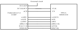
Figure 4 FPGA and DSP hardware connection diagram
2.2.2 DSP software writing
As a signal processing chip, DSP has a strong advantage in processing various signals. In this system, most image processing algorithms (car license plate location, segmentation, character recognition, etc.) are implemented on it. After building a good hardware platform, the next thing to do is to write the DSP. There are two main programs written here: algorithm migration and underlying driver development.
CCS (Code Composer Studio) is an integrated development environment launched by TI to develop TI's DSP chip applications. The DSP/BIOS [8] integrated in CCS is TI's C5000 series and C6000 series digital signals. An embedded real-time operating system kernel tailored to the processing chip has the advantages of graphical interface, code rapid prototyping function and complete API function library, which can greatly facilitate application system development and online debugging. This system uses the DSP/BIOS operating system that comes with CCS2.2 to develop the program. It uses a series of programming tasks, threads, semaphores, mailboxes, etc. to conveniently control the real-time scheduling of the program.
(1) Algorithm migration: The general algorithm is written on Matlab. Although it is a C-like language, it still has many differences compared with the standard C, and Matlab often provides various signal processing tools. Such as image processing, neural networks, wavelet transforms, and so on. We simply call these functions and bring in several parameters to facilitate various signal processing. Therefore, when these algorithms are transplanted into the DSP of this system, some functions have to be rewritten, and the programming format and style have to be changed. In some places, in order to improve the efficiency of the algorithm and make full use of DSP resources, it should also be Write some code into assembly language and more. When the entire algorithm is transplanted, it is finally encapsulated into a function, which makes it easier to maintain and call the entire algorithm. Then, when the trigger condition is met, the algorithm processing function is called by a certain task in the DSP/BIOS to complete the recognition of the license plate image.
(2) Development of the underlying driver: The underlying driver is written using the CSL (Chip Support Library) provided by CCS for the underlying driver development. CSL provides a series of application programming interfaces (APIs) for configuring and controlling the DSP on-chip. Peripherals simplify the development of DSP on-chip peripherals and greatly shorten the development cycle.
2.3 FPGA function module
FPGA is the abbreviation of English Field Programmable Gate Array, which is a field programmable gate array. It is a product of further development based on programmable devices such as PAL, GAL and EPLD. The use of FPGAs is very flexible, and the same FPGA can generate different circuit functions through different programming data. FPGAs are widely used in communications, data processing, networking, military, and aerospace.
In the design of this system, FPGA plays a very important role as the core module of image acquisition, storage and transmission, coordinating and controlling the normal operation of the whole system. This system selects the EP1C12Q240 model FPGA in the Cyclone series of Altera's cost-effective. The FPGA has a total of 52 memory blocks for a total of 239,616 bits. Each block can be configured into different storage modes, such as single-port RAM, simple dual-port RAM, shift register, ROM and FIFO, through the built-in MegaWizard tool of QUARTUS II, which is beneficial for the system to temporarily store images when acquiring images. Data and design of the FPGA as SBSRAM for DSP access. The FPGA has enough IO ports on the chip to leave room for future expansion of the system.
The devices connected to the FPGA here are: SAA7113H, SDRAM, DSP, and MAX3232. Since the FPGA is purely a programming device, its IO pin can be configured to any signal we need, and can be connected to any interface, so the hardware interface is relatively simple to design. The difficulty lies in writing various communication protocols and different interfaces for seamless transmission. The overall FPGA programming diagram is shown in Figure 5: The parts inside the block are the various modules of the FPGA and the interconnections between them. The part outside the box is the peripheral device of the FPGA.
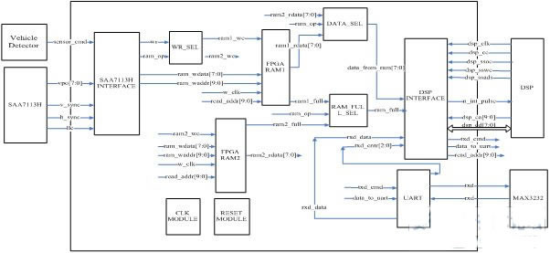
Figure 5 Overall block diagram of the FPGA programming
The FPGA system functions as an image acquisition, buffering, and transmission function throughout the license plate recognition system. When the sensing signal sensor_cmd signal of the vehicle detector is valid, the state machine inside the SAA7113H_INTERFACE module is started to perform image collection. When the SAA7113H_INTERFACE module detects the field start signal from the SAA7113H video stream, one frame of image data is transmitted. Since the video stream is PAL, one frame of image is divided into two fields of image data of odd field and even field.
The system adopts the design method of ping-pong structure. This typical design method is often applied in the FPGA design method of “area change rateâ€. Since there are 52 memory blocks in the EP1C12Q240C8, a total of 239,616 bits, it is feasible to design a small amount of RAM inside the FPGA. Two 720*8bits (image data size per line) space are designed in the system. The write clock signals of these two memories are twice the output clock LLC of the SAA7113H. The SAA7113H INTERFACE module collects the Y component of the standard YUV 4:2:2 through the VPO bus connected to the SAA7113 (only the Y component is acquired to obtain the grayscale image), that is, the luminance signal therein, and the image of one line contains 720 luminance information. The bit width of the luminance information is 8 bits. When the image line of FPGA_RAM1 is full, the line full signal ram1_full is sent to the DSP_INTERFACE module, and the signal is converted to the interrupt signal n_int_pulse in the DSP_INTERFACE module to notify the DSP to call EDMA to acquire the image of the line. At the same time, the internal RAM is switched, and the next row of data is written into the FPGA_RAM2 to ensure that one DSP reads one line of image data, while the FPGA writes the next line of image data to another RAM to complete a ping-pong operation.
After the DSP completes the processing of the license plate image, the recognition result of the license plate image is written back to the internal register of the DSP_INTERFACE module of the FPGA through EMIF, and the values ​​of these registers are obtained through the UART module, and transmitted to the PC through the UART.
The waveform shown in Figure 6 is the simulation waveform of one of the SAA7113_INTERFACE modules on the Modelsim in the internal block diagram of Figure 5. It is seen from the simulation waveform that it is consistent with the actual SAA7113 output waveform and achieves our expected results.
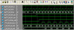
Figure 6 SAA7113_INTERFACE simulation waveform
3. Conclusion
The embedded license plate recognition system based on DSP and FPGA designed in this paper has the characteristics of high speed, high stability, small size and low power consumption. It provides a good verification platform for license plate recognition algorithm, as shown in Figure 7. After verification, the license plate recognition system can realize real-time image acquisition, transmission and recognition. From the perspective of time, it takes less than 400ms to complete the processing (positioning, normalization, feature extraction and coding) of a single license plate image in the DSP. The speed is very fast; from the recognition rate, as long as The algorithm meets certain requirements. After the license plate recognition system is operated, the recognition rate can also be very high. In short, the system has certain application value in license plate recognition.
Finally, as a practical license plate recognition system, in the future system design, it is also necessary to add parts for network communication, and some more intelligent functions, such as liquid crystal display, voice prompts and the like. In short, the embedded license plate recognition system is one of the important research topics in the field of intelligent transportation applications, and has broad application prospects.
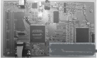

Figure 7 physical map of the license plate recognition system
references
[1] Chen Youren. Research on automatic recognition of license plates in images [D]. Shanghai: Shanghai Jiaotong University, 2001: 1-10.
[2] Liu Ling, Zhang Xinghui. Research on Intelligent License Plate Recognition System[J]. Journal of Scientific Instrument, 2004, 25(4) Supplement: 565-567.
[3] Su Housheng. Design and Implementation of License Plate Recognition System[J]. Machine Vision, 2006, (3): 103-107.
[4] Hong Jian, Chen Jirong. Design of real-time license plate recognition system based on DSP+CPLD[J]. Journal of Computer Applications, 2007, 24(7): 218-219.
[5] Kong Xianggang, Zhu Jing, Yang Tao. Application of SAA7113H in Video Acquisition Interface Design[J]. Electronic Technology, 2003, (12): 26-29.
[6] Zhang Zhanpeng, Su Xiuqin, Lv Shuaihua. Control Implementation of SAA7113H Based on TMS320C620X Series DSP[J]. Science Technology and Engineering, 2006, 6(12): 1693-1695.
[7] Li Fanghui, Wang Fei, He Peiyu. Principles and Applications of TMS320C6000 Series DSPs [M]. Beijing: Publishing House of Electronics Industry, 2005: 337-380.
[8] Song Shengli, Zeng Wei. Application of DSP/BIOS in Digital Image Processing[J]. Foreign Electronic Measurement Technology, 2005,24(12):33-36.
The accessories are very important in using and installing, so we offer the driver,controller,Mounting Brackets,and led strip caps.Use the driver to support the led strip lights,because the led strips are low voltage. If there needs color change or adjusting brightness,the RGB controller or dimmer can make it real.In order to make the installation easy, the unique brankets are optional.Each evenstrip has matched bracket.If the length of led strip needs to cut short,use the plastic end caps to keep waterproof.
Strip Light Accessories,Waterproof Led Driver,Led Strip Light Controller,Led Strip Cap
Guangdong Kamtat Lighting Technology Joint Stock Co., Ltd. , http://www.ip68ledstrip.com