design background:
Random access memory (random access memory, RAM), also known as "random memory", is an internal memory that directly exchanges data with the CPU, also called main memory (memory). It can read and write at any time, and it is very fast, usually used as a temporary data storage medium for the operating system or other running programs.
The contents of the storage unit can be taken out or stored as needed, and the access speed is independent of the storage unit's location. This kind of memory will lose its storage contents when the power is turned off, so it is mainly used to store programs for short time use. According to the working principle of the storage unit, the random access memory is divided into static random access memory (English: Static RAM, SRAM) and dynamic random access memory (English Dynamic RAM, DRAM).
Â
Design principle : Â
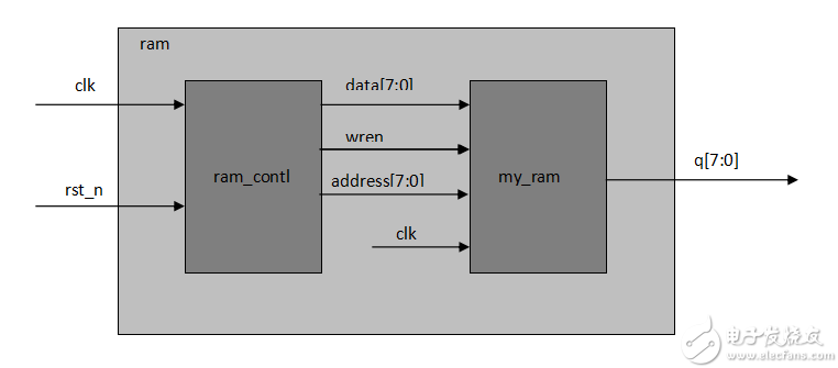
In this design, we call our RAM's IP core to write it to our controller to achieve the readable and writable characteristics of RAM.
What we designed is the depth of RAM is 256, we write 256 numbers first, then read out the 256 numbers we wrote. It is worth mentioning that our read and write flags are the high bit for the write flag and the low bit for the read flag.
Design steps, open our interface to call the IP core, and then the next step:
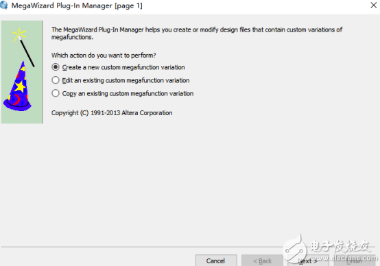
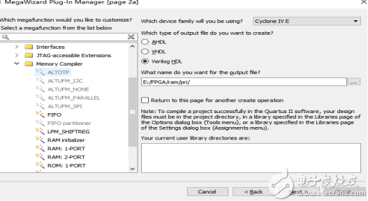
    Select our RAM in the following options , as shown in the figure, and then give us an output name, and then the next step:
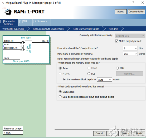
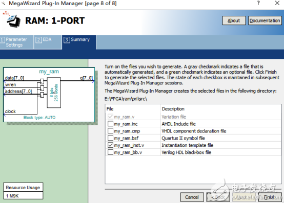
In the following page we set our bit width and depth, then set as follows, the next step:
    On the following page, ask us to set whether to set our output register, we do not set it, as follows, and then the next step:
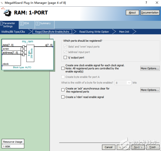
Then the next step, the next step, directly to the following interface, choose to generate. Inst file, and then complete.
Â
Design architecture diagram :
Design code :
Top-level module
0 Â module ram ( clk , rst_n , q ); // Input and output port settings
1 Â input clk ;
2 Â input rst_n ;
3 Â
4  output  [ 7 : 0 ] q ;
5 Â
6  wire  [ 7 : 0 ] data ;
7 Â wire wren ;
8  wire  [ 7 : 0 ] address ;
9 Â
10 ram_contl ram_contl ( // Instantiate our RAM controller
11. Clk (clk),
12. Rst_n (rst_n),
13. Data (data),
14. Wren (wren),
15. Address (address)
16 );
17 my_ram my_ram_inst ( // Instantiate ip core
18. Address (address),
19. Clock (clk),
20. Data (data),
21. Wren (wren),
22. Q (q)
23 );
twenty four  endmodule Â
Â
Design module
0 Â module ram_contl ( clk , rst_n , data , wren , address );
1 Â input clk ;
2 Â input rst_n ;
3 Â
4  output  reg  [ 7 : 0 ] data ; // output
5  output  reg wren ; // Read and write bits
6  output  reg  [ 7 : 0 ] address ; // address bit
7 Â
8 Â reg state ;
9  always  @ ( posedge clk or  negedge rst_n )
10 if (! Rst_n )
11 begin
12 data  8'b0 ;
13 wren  1'b0 ;
14 address  8'b0 ;
15 state  1'b0 ;
16 end
17 else
18 begin
19 case  ( state )
20 0 : begin
21 wren  1'b1 ; // Turn on write enable, write our data
22 if ( address  255 )
23 begin
24 address address + Â 1'b1 ; Â // Add one address,
25 data data + Â 1'b1 ; Â Â Â Â Â // Data plus one
26 end
27 else
28 begin
29 address  1'b0 ; // Open reading after writing
30 data  1'b0 ;
31 state  1 ;
32 wren  1'b0 ;
33 end
34 end
35 1 : begin
36 if ( address  255 )  // Read our data
37 begin
38 address address + Â 1'b1 ;
39 end
40 else
41 begin
42 address  1'b0 ;
43 state  0 ;
44 end
45 end
46 default : state  0 ;
47 endcase
48 end
49 Â endmodule Â
Â
Test module
0  `timescale  1ns / 1ps
1 Â
2 Â module ram_tb ();
3 Â reg clk ;
4 Â reg rst_n ;
5 Â
6  wire  [ 7 : 0 ] q ;
7 Â
8  initial  begin
9 Â clk = Â 1'b1 ;
10 rst_n = Â 1'b0 ;
11
12 # 100.1 rst_n = Â 1'b1 ;
13
14 # 200000.1 Â $ stop ;
15
16 end
17
18 always  # 10 clk =  ~ clk ;
19
20ram ram_dut (
As a mobile multi-purpose platform, tablet computers also provide many possibilities for mobile teaching. The touch-based learning & entertainment teaching platform allows children to efficiently improve their academic performance in a relaxed and pleasant atmosphere. Such tablet computers generally integrate two learning sections of various courses and systematic learning functions. Generally, it includes multi-disciplinary high-quality teaching resources. The education tablet has the following main functions: it has the functions of touch screen input, text editing, picture editing, data storage, data management, wired and wireless Internet access that ordinary tablet computers have; Management functions, search methods support manual search, query by keyword, query by time; text and pictures can be scanned and converted into documents to save.
Education Tablet,learning tablet,leaning machine,New learning tablet
Jingjiang Gisen Technology Co.,Ltd , https://www.jsgisengroup.com