A single test circuit can be used at that time, but today is not the case because modern op amps have a more comprehensive specification. Therefore, a single test circuit no longer covers all DC tests.
Workbench and production tests are now performed on the op amp DC parameters using three test circuit topologies. These three topologies are (1) dual op amp test loops, (2) self-test loops (sometimes called fault summing point test loops), and (3) triple op amp loops. You can use these circuits to test DC parameters, including quiescent currents ( ![]() ), voltage imbalance (
), voltage imbalance ( ![]() ), power supply rejection ratio (PSRR), common mode rejection ratio (CMRR), and DC open loop gain (
), power supply rejection ratio (PSRR), common mode rejection ratio (CMRR), and DC open loop gain ( ![]() ).
).
Quiescent Current
The quiescent current is the current consumed by the device when the output current is equal to zero. in spite of ![]() Testing seems fairly straightforward, but care must also be taken to ensure good results, especially when dealing with extremely high or low
Testing seems fairly straightforward, but care must also be taken to ensure good results, especially when dealing with extremely high or low ![]() When the part is. Figure 1 is available for testing
When the part is. Figure 1 is available for testing ![]() Three practical circuits for other parameters, which must take into account several load current conditions. This includes the feedback current in the test loop. In fact, feedback resistor
Three practical circuits for other parameters, which must take into account several load current conditions. This includes the feedback current in the test loop. In fact, feedback resistor ![]() Can also bring load to the device, affecting
Can also bring load to the device, affecting ![]() measuring.
measuring.
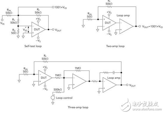
Figure 1. These three circuits can be used to measure quiescent current ( ![]() ).
).
Let's take a test of the OPA369 op amp as an example to illustrate these circuits. The maximum quiescent current of this part is 1μA per channel. The maximum input offset voltage is 750μV. The dual op amp loop circuit in Figure 1 provides 750.75mV for the output of the device under test. This input voltage can make ![]() Pass 15μA of current. This current comes from the power supply and adds an error to any measurement. So proceeding
Pass 15μA of current. This current comes from the power supply and adds an error to any measurement. So proceeding ![]() Before measuring, measures must be taken to ensure that the output current is really equal to zero.
Before measuring, measures must be taken to ensure that the output current is really equal to zero.
The self-test circuit is not the most efficient circuit for measuring very low quiescent current because the output must provide feedback current. In this implementation, the output must be offset according to the voltage after the gain ![]() Adjust (not easy) or disconnect the 50Ω resistor from the schematic above to eliminate the feedback current. A dual amplifier loop can achieve zero output by adding another amplifier. Careful selection of low input bias current loop amplifiers results in very small output current errors.
Adjust (not easy) or disconnect the 50Ω resistor from the schematic above to eliminate the feedback current. A dual amplifier loop can achieve zero output by adding another amplifier. Careful selection of low input bias current loop amplifiers results in very small output current errors.
In addition, the three op amp loops can also help you measure ![]() However, pay attention to the 1MΩ resistor at the output of the device being measured. This will be a problem because it is always a parasitic load regardless of which parameter is measured. If the output load current is measured, the resistor represents an additional load. In addition, the noise problem of this resistor must be considered. The noise of a 1MΩ resistor is 85μVp-p at a frequency of 0.1Hz to 10kHz. Use a 100kΩ resistor to reduce the noise to 27μVp-p. Therefore, lowering the resistor value reduces noise, but the parasitic resistor load at the output of the device being measured is then more pronounced.
However, pay attention to the 1MΩ resistor at the output of the device being measured. This will be a problem because it is always a parasitic load regardless of which parameter is measured. If the output load current is measured, the resistor represents an additional load. In addition, the noise problem of this resistor must be considered. The noise of a 1MΩ resistor is 85μVp-p at a frequency of 0.1Hz to 10kHz. Use a 100kΩ resistor to reduce the noise to 27μVp-p. Therefore, lowering the resistor value reduces noise, but the parasitic resistor load at the output of the device being measured is then more pronounced.
Voltage offset
![]() Testing is the basis for measuring most of the other DC technical parameters of an op amp. Therefore, pay special attention to the test circuit to ensure that the circuit works well when testing other parameters. If the test configuration is not selected, it will affect other DC measurements.
Testing is the basis for measuring most of the other DC technical parameters of an op amp. Therefore, pay special attention to the test circuit to ensure that the circuit works well when testing other parameters. If the test configuration is not selected, it will affect other DC measurements.
![]() There are several ways to define it, including: “Differential DC input voltage required to provide zero output voltage when there is no input signal or no supply resistance†(Reference 2), or “No in any input to ground path†The differential DC input voltage required to provide zero output voltage when other input signals and resistors are zero" (Reference 3). Another definition is “differential DC input voltage required to provide zero voltage at the op amp output when the input bias current is zeroâ€, which is an ideal theoretical method for measuring the input offset voltage and is not practical because An op amp with zero input bias current does not exist.
There are several ways to define it, including: “Differential DC input voltage required to provide zero output voltage when there is no input signal or no supply resistance†(Reference 2), or “No in any input to ground path†The differential DC input voltage required to provide zero output voltage when other input signals and resistors are zero" (Reference 3). Another definition is “differential DC input voltage required to provide zero voltage at the op amp output when the input bias current is zeroâ€, which is an ideal theoretical method for measuring the input offset voltage and is not practical because An op amp with zero input bias current does not exist.
According to the above definition, you can connect a low-output, high-precision, high-resolution variable voltage power supply to the input of the operational amplifier, or adjust the input voltage until the output voltage is zero. Then the input offset voltage is simply the inverse of the applied input voltage.
There are two serious problems with this approach. When testing an op amp with a very high open-loop gain, you must ensure that the resolution of the voltage supply is less than 1 microvolt to ensure any degree of repeatability. In addition, iterative proximity must be used to make the output voltage zero. The noise in the system is coupled into the voltage supply and the operational amplifier, making measurement and control in a high-speed automated test environment almost impossible.
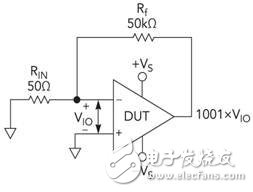
Figure 2. Using this circuit to measure voltage offset ![]() .
.
Due to these problems with the ideal method, the common method chosen in the bench test environment is to place the device under test in an inverting gain configuration, as shown in Figure 2. The advantage of this approach is that not only is the device under test very stable, but usually no additional compensation is required.
In addition, the test circuit may also need to provide a 50Ω resistor between the non-inverting input and ground to offset the input bias current. However, for an op amp with a very low input bias current, the only real "contribution" of the resistor is to increase the noise. For a 100pA device, the additional error is 0.005μV without this resistor. This cancellation only works when the direction and magnitude of the bias current are equal.
The circuit in Figure 2 is a simplified representation of the self-test summing point method in Figure 1, but without resistors R1 and R2. This circuit has inherent stability for most op amps and can often overwhelm any potential deficiencies, making it the preferred test circuit.
If you use the test circuit in Figure 2 for other tests, the shortcomings will appear. For example, the circuit in Figure 2 will measure ![]() with
with ![]() Other parameters affect the impact.
Other parameters affect the impact.
This undriven circuit can cause ![]() Error, the error value is equal to (
Error, the error value is equal to ( ![]() * Closed loop gain)*
* Closed loop gain)* ![]() (The unit is V/V). This error may not matter, or it can be done by applying the appropriate VIN
(The unit is V/V). This error may not matter, or it can be done by applying the appropriate VIN ![]() Reduced by 0.0V.
Reduced by 0.0V.
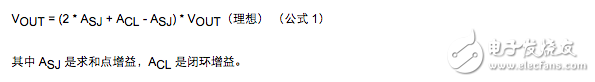
The output error compensation formula for the desired output can be adjusted using Equation 1 below.
An additional amplifier can usually be used in the test loop, as shown in the dual amplifier loop of Figure 1. This configuration is the closest ![]() Defined requirements. The output of the device under test remains in the loop amplifier to ground
Defined requirements. The output of the device under test remains in the loop amplifier to ground ![]() within. If the loop amplifier supports V regulation, or you can eliminate the offset by controlling the non-inverting input, you can ignore the loop amplifier's offset. In this way, you can make the output of the device under test zero. in
within. If the loop amplifier supports V regulation, or you can eliminate the offset by controlling the non-inverting input, you can ignore the loop amplifier's offset. In this way, you can make the output of the device under test zero. in ![]() The measured voltage is 1001*
The measured voltage is 1001* ![]() . Unless a load is connected to the output of the device under test, the output must only provide the loop amplifier input bias current. This is low for measuring quiescent current
. Unless a load is connected to the output of the device under test, the output must only provide the loop amplifier input bias current. This is low for measuring quiescent current ![]() It is an important consideration for components. In the previous two circuits, the device under test must provide feedback current to
It is an important consideration for components. In the previous two circuits, the device under test must provide feedback current to ![]() .
.
By connecting the non-inverting input of the loop amplifier to a programmable voltage supply, you can measure other performance parameters of the op amp, such as ![]() , output swing and CMRR. Since the loop control voltage is varied, the output of the device under test attempts to match the control voltage.
, output swing and CMRR. Since the loop control voltage is varied, the output of the device under test attempts to match the control voltage.
Note that the dual amplifier loop has the following disadvantages:
More complicated than self-testing circuits;
Loop compensation is required because the circuit itself is not stable;
The output of the device under test can only be controlled within the common mode range of the loop amplifier.
If the loop is not properly compensated, the circuit will oscillate. You can pass ![]() Connect a suitable capacitor in parallel to stabilize the loop. Arranging the appropriate RC combination for the loop amplifier also stabilizes the loop. We will explore this loop compensation problem in a future article.
Connect a suitable capacitor in parallel to stabilize the loop. Arranging the appropriate RC combination for the loop amplifier also stabilizes the loop. We will explore this loop compensation problem in a future article.
One variation of the dual amplifier loop test method is a three-amplifier loop that provides current control of the output voltage of the device under test. The compensation for this loop can be set by the RC combination of the second loop amplifier. As in the dual op amp circuit, the voltage offset of the device under test is also ![]() Measurement, and
Measurement, and ![]() It is 1001 times the voltage offset. This circuit topology solves the problem of output swing limitation of the device under test of the former circuit. If a larger output swing is required, the resistor in series with the loop control voltage can be reduced.
It is 1001 times the voltage offset. This circuit topology solves the problem of output swing limitation of the device under test of the former circuit. If a larger output swing is required, the resistor in series with the loop control voltage can be reduced.
Note that the three amplifier loops have the following disadvantages:
More complicated than other circuits;
Loop compensation is required because the circuit itself is unstable;
The output of the device under test always has a minimum load of 1 MΩ.
Power supply rejection ratio
PSRR is the ratio of the absolute value of the supply voltage change to the change in the op amp input offset voltage. Simply put, it is the ability of an op amp to suppress supply voltage variations over a specific range. Since the offset voltage is required to complete the measurement, you can measure using existing technology ![]() . The three test loops in Figure 1 can be used to complete PSRR measurements. The method is to set the power supply +VS and -VS to the lowest supply voltage of the device under test, and measure 1001*
. The three test loops in Figure 1 can be used to complete PSRR measurements. The method is to set the power supply +VS and -VS to the lowest supply voltage of the device under test, and measure 1001* ![]() . Next, set the power supply voltage to the maximum voltage of the device under test, and then measure 1001* again.
. Next, set the power supply voltage to the maximum voltage of the device under test, and then measure 1001* again. ![]() . Equation 2 and Equation 3 are the calculation methods for PSRR.
. Equation 2 and Equation 3 are the calculation methods for PSRR.

Some op amps need to consider other factors when using this method. These op amps have low enough operating voltages, and the midpoint of the supply (zero common-mode voltage) can exceed the maximum common-mode voltage allowed by low-power op amps. Some rail-to-rail input devices have multiple input stages that operate smoothly under these conditions, but they convert to different input stages, resulting in PSRR calculation errors. In both amplifiers, the fixed common-mode voltage prevents common-mode saturation or input-level conversion. Maintaining a constant common-mode voltage for these two measurements of the PSRR test produces an error that can be cancelled during the PSRR calculation. The actual common-mode voltage required for these devices will vary depending on the topology of the amplifier's input stage.
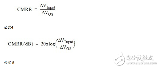
Common mode rejection ratio
CMRR is the ratio of differential voltage gain to common mode voltage gain, which is the ability of an op amp to reject common-mode voltages within a specified range. Since the measurement is done by the demand offset voltage, you can use the existing one. ![]() Measurement techniques to measure CMRR.
Measurement techniques to measure CMRR.
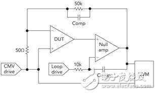
Figure 3. This dual amplifier loop helps you measure the CMRR of your op amp.
During this test, the input common-mode voltage needs to be changed and the op amp measured ![]() The change. The most obvious method is to apply the common mode voltage to the non-inverting input of the device under test. This method requires the measurement system to be referenced to the applied common mode voltage. Figure 3 shows the test setup for a dual amplifier loop.
The change. The most obvious method is to apply the common mode voltage to the non-inverting input of the device under test. This method requires the measurement system to be referenced to the applied common mode voltage. Figure 3 shows the test setup for a dual amplifier loop.
If you wish to complete all measurements related to grounding, connect the non-inverting input to ground and move the power supply in a forward or negative direction in a tracking manner to apply an effective common-mode voltage to the amplifier. The output must be at the midpoint of the power supply to eliminate the effects of CMRR measurements ![]() error. Equation 4 and Equation 5 are the calculation methods for CMRR.
error. Equation 4 and Equation 5 are the calculation methods for CMRR.
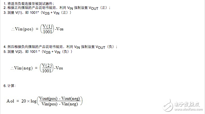
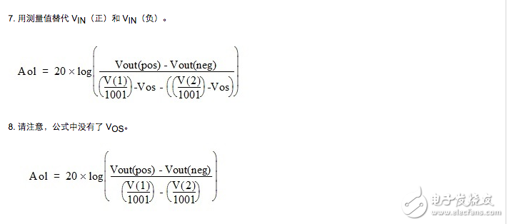
DC open loop gain
![]() Is the ratio of the output voltage to the differential input voltage. This measurement requires measuring the input offset voltage at multiple points and calculating the AOL.
Is the ratio of the output voltage to the differential input voltage. This measurement requires measuring the input offset voltage at multiple points and calculating the AOL.
measuring ![]() You need to know the output behavior of the op amp being measured. Ideally, the op amp may swing to both power rails. This is not the case.
You need to know the output behavior of the op amp being measured. Ideally, the op amp may swing to both power rails. This is not the case. ![]() There is a certain distance from the rail under a given load.
There is a certain distance from the rail under a given load.
Assume that the output is available from ![]() (positive) swing to
(positive) swing to ![]() (negative). If the output is reached
(negative). If the output is reached ![]() (Positive), the voltage at the input of the device under test will be
(Positive), the voltage at the input of the device under test will be ![]() +
+ ![]() (positive). Need extra voltage
(positive). Need extra voltage ![]() (positive) drive output to
(positive) drive output to ![]() (positive). Instead, if the output is reached
(positive). Instead, if the output is reached ![]() (negative), the voltage at the input of the device under test will become
(negative), the voltage at the input of the device under test will become ![]() +
+ ![]() (negative). You need to measure this change at the input to achieve the desired full-scale output.
(negative). You need to measure this change at the input to achieve the desired full-scale output.
Measure using Figure 1 ![]() The method is:
The method is:
In a future article, we will introduce the input bias current test conditions and error sources that need to be considered when designing and testing an operational amplifier. We will provide a test circuit that you can use to integrate the self-test circuit with the dual amplifier loop to take advantage of both test methods. The third article will introduce the compensation problem because the double amplifier loop will oscillate without proper compensation.
For the SMD LED 495nm LED,
we can supply dual-chip blue LED, three-chip cyan LED, multi-chip cyan LED, high voltage LED, flashing cyan LED and variety of size SMD LED. For instance: 3528 SMD cyan 490nm LED, 3528 SMD cyan 495nm LED, 3528 SMD cyan 500nm LED. 2835 SMD cyan 490nm LED, 2835 SMD cyan 495nm LED, 2835 SMD cyan 500Nm LED .
There are also have many other shapes to choose, like the 5050 SMD cyan LED, the 5730 SMD cyan LED ect. You can choose any one of them for your requirement.
We supply variety of 490nm LED products. Including Through-hole 490nm LED, SMD 490nm LED and high-power 490nm LED. We can also produce 490nm LED according to your requirement.
For the Through-hole Light Emitting Diode 490nm cyan LED,
we can customize the shape, the lighting angle, the number of emitting source, the flat pin LED and braided LED. Such as: 5mm cyan 490nm LED, 5mm cyan 495nm LED, 5mm cyan 500nm LED, 5mm cyan 505nm LED, 5mm cyan 510nm LED. 3mm cyan 490nm LED, 3mm cyan 495nm LED, 3mm cyan 500nm LED, 3mm cyan 505nm LED, 3mm cyan 510nm LED ect.
There are many other shapes for your choose. Customized cyan LED are available
490nm led is a aqua blue LED. Common aqua blue LEDs are like: cyan 490nm LED, cyan 490nm LED, cyan 490nm led and so on.

We will do the High temperature resistance testing and 10 hours ageing treatment before the product out off the factory, which can ensure the stability of each product.
Our LED products have 5 year warranty.
We are the best supplier for your light-emitting diode.
495nm LED
495nm LED,490nm LED,495nm Green LED,495nm 3w LED,495nm LED Lights
Shenzhen Best LED Opto-electronic Co.,Ltd , https://www.bestsmd.com