This article aims to introduce some of the test principles and system principles behind the UMTS test project through some of the UMTS test cases. I hope everyone can learn about the system principles and test principles behind some test projects.
1. OverviewThis paper mainly introduces the testing principle of some important test items for the UMTS terminal RF test specification, and mainly introduces the RF test items specified in the TS34.121 specification. Since the UMTS specification has evolved from R99 to protocol versions such as R5, R6, R7, R8, and R9, the basic structure of the physical layer such as the channel structure has changed greatly. Therefore, for the same test item, such as maximum power test, the specification is for different versions. The terminal also defines different subtest items. For example, the maximum power test defines several test items such as 5.2, 5.2A, 5.2AA, and 5.2B. The complexity of UMTS testing is also due to the latency of the processes and channels between these channels.
This article takes several basic UMTS test projects as examples to try to express the system principles and test principles behind these test items.
1.1. Selection of trigger mode
The following two descriptions are often seen in the specification, as described in 5.2A:
The maximum output power with HS-DPCCH is a measure of the maximum power the UE can transmit when HS-DPCCH is fully orparTIally transmitted during a DPCCH TImeslot.
Description in 5.2B:
The maximum output power with HS-DPCCH and E-DCH is a measure of the maximum power the UE can transmit when HS-DPCCH and E-DCH is fully or parTIally transmitted during a DPCCH TImeslot.
The meaning of the two paragraphs is that we are required to do the TX test, referring to Figure 4.1, we can see that the HS-DPCCH and E-DCH transmissions have discontinuous characteristics, so we are required to transmit when the two channels are activated. At this time, the radio performance of the relevant channel activation can be verified. Therefore, the description of the above specification becomes a problem of finding the corresponding uplink physical channel. The answer to this question can be found in 3GPP TS 25.211 7.7.
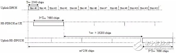
Figure 1.1, Upstream Channel Time Relationship
According to the description in Figure 1.1, the time difference between the uplink HS-DPCCH and the uplink DPCH is m*256 chips, which is recorded as T1.
Where m = (TTX_diff/256) + 101, the delay is approximately 1024 chips in the CMU 200. The time difference between the uplink DPCH and the downlink DPCH is the air interface delay of the DPCH in the channel transmission, which is denoted as T2, and the delay between the downlink DPCH and the CPICH is T_dpch_offset, which is denoted as T3, and the parameter is in units of 256 chips, in the CMU 200 and Both can be configured directly in the CMW500. Therefore, the delay of the uplink HS-DPCCH and the CPICH is T1+T2+T3.
The comprehensive tester will find the uplink HS-DPCCH channel within a certain range according to the downlink frame boundary, that is, the time of the CPICH channel and the parameters of a series of systems. After the first HS-DPCCH is fixed, since the period of the channel is 12 ms, the actual occurrence time of the HS-DPCCH channel can be determined later by time.
In the actual operation, you can select HS-DPCCHTrigger directly in the comprehensive tester! The principle of E-DCH is similar to the principle of HSDPA, which is not described in detail here!
1.2, dynamic terminal power test
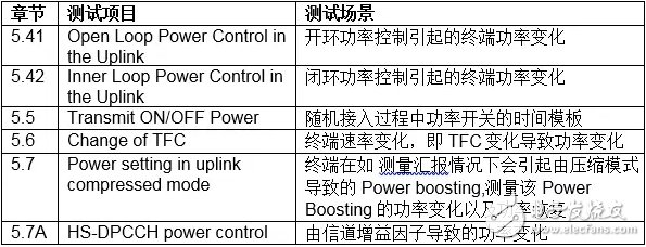
In the LTE system, the characteristics of some systems may cause changes in terminal power, such as TFC changes (including DTX), Power Boosting in compressed mode, PRACH access in open loop power control, and TPC response of DPCH in closed loop power control. Channel gain factor changes, etc. For the power change process of UMTS, the 3GPP TS34.121 specification has developed a response test item, as shown in Table 1.1:

About this item
- 9V Switching wall charger
- 110V input voltage / 9VDC 1A/2A/3A... output voltage
- For use with Arduino Uno, Mega and MB102 Power supply boards
- Connector size: 5.5 x 2.1mm/5.5*2.5mm...
- Center or Tip is positive, sleeve is negative
9v wall charger,AC Power Supply Wall Plug,Wall Adapter Power Supply,9V Power Adapter,ac 50/60hz power adapter,Wall Adapter Power Supply - 9VDC,100-240v converter switching power adapter
Shenzhen Waweis Technology Co., Ltd. , https://www.szwaweischarger.com