Since the generation of external lighting, we have divided lighting into three eras: the filament bulb era (incandescent lamp), the gas bulb era (fluorescent lamp), and the semiconductor light-emitting era (LED). Among them, the longest history of incandescent lamps and future mainstream LEDs are the most important points of investigation. Regardless of the development of the times, the production process of the lighting industry is strikingly similar, except that China is in the downstream of the industry. The core technology is basically owned by countries such as Europe, America and Japan.
1. The principle of LED lighting is that when electrons pass through a layer of semiconductor material, the semiconductor material is excited to convert electrical energy into light energy. However, the light-emitting ability of a single-layer semiconductor is very weak, so many layers of single-layer materials should be superimposed and pressed into a composite material like a thousand-layer cake.
Therefore, the luminous efficiency of LED depends on how many layers can be pressed in the same thickness. The thinner the single-layer material, the more layers can be stacked, and the higher the luminous efficiency. Now the thickness of each layer is generally only 2-20 microns, which also determines that the epitaxial wafer production is the most difficult part of the entire LED production process.
2. Cutting-LED core: It is equivalent to extracting the filament from the tungsten wire material. The difference is that the cut epitaxial wafer is square.
Due to the special structure of the epitaxial wafer, it is very difficult to cut the light-emitting core intact. Not only need a vacuum environment, but also a professional cutting machine. At present, only two manufacturers in the world produce this cutting machine.
3. Put the core into the LED chip: the chip is to the LED, just like the lamp holder is to the light bulb, it is the power supply part. "Chip" is very important equipment to achieve the ideal effect of LED, because LED has very high requirements on current.
4. Encapsulate the LED chip into a luminous body: encapsulate the LED chip into a luminous body, just like adding a lampshade to a filament lamp holder to make a light bulb. The shape of the lampshade can be different according to the needs, but the packaging technology determines the service life of the luminous body.
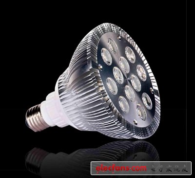
5. Lighting application: Just like using incandescent bulbs, according to different functions and needs, assembled into different LED products.
For LED lighting, the first three steps of epitaxial wafers, dicing and chips are upstream, the fourth step of packaging is midstream, and the fifth step of application is downstream. These problems require us to use more energy to break through.
Light-resistant design ,and support single and muilt touch points,widely use to financial telecom service,Adverstisement show,Industrial control ,public query ,self-service,E-education ,and games etc aera.Ultra-thin, ultra-narrow design, no matter whether it is external or built-in, it can adapt to various needs without affecting the appearance and saving built-in space. Infrared sensing principle, simple finishing, LED die, stable performance, high touch precision and long life.The unique installation method makes the installation of the client a breeze.The surface of the aluminum alloy is sprayed and oxidized, and the whole is delicate, simple, generous and multi-touch. Simple operation, USB connection, plug and play.
Picture show:


Diy Infrared Touch Frame,Infrared Touch Screen Kit,Install Infrared Touch Frame,Ir Touch Frame Diy,Usb Infrared Touch Screen,Outdoor Infrared Touch Screen
ShenZhen GreenTouch Technology Co.,Ltd , https://www.bbstouch.com