Tag: Silicon Crystal Semiconductor CMOS
This article refers to the address: http://
The optimization of the layout of silicon semiconductor components has become the key to minimizing chip area. This strategy increases the number of chips per wafer and thus achieves a minimum unit cost. Since a CMOS image sensor must be combined with a lens train to complete a solid-state camera module, the development of a CMOS image sensor depends on different economic considerations. In order to achieve the smallest size of the camera module, the silicon layout must be traded off to reduce assembly costs and increase product reliability through package innovation.
Solid state image sensor
Solid-state image sensors are being widely used in various products. In terms of quantity, the largest application market in the current mobile phone camera module, this year alone for this application, there are more than two million per day.
Most solid-state image sensors are based on CMOS technology because CMOS technology offers a more integrated approach than charge coupled device (CCD) technology. The CMOS image sensor includes a 2D array of solar cells that provide photoelectric conversion and many other electronic modules for image, interface and power management.
Non-optimized silicon crystal design
Since the CMOS chip layout is not affected by the need to maximize wafer utilization, it is perhaps a unique semiconductor component. For a typical semiconductor component, the chip layout typically must maximize the number of chips per wafer to minimize the unit manufacturing cost of the chip. However, image sensors are just one of the components required for camera modules. Other key components include lens modules, adjustable lens housings, infrared filters, carrier boards, and passive components and decoupling capacitors that are often used. Figure 1 is a relative cost comparison table for a typical 1.3M pixel camera module assembly. Since the cost of optical components has exceeded the cost of other semiconductor components, a compromise between silicon layout and optical design has to be driven by product cost and size requirements.
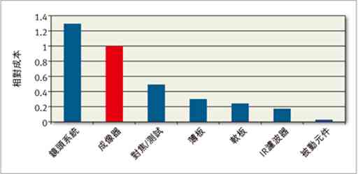
Figure 1: The relative cost of the main components of a solid-state camera module, usually based on an image sensor chip
First generation image sensors are typically manufactured following standard semiconductor principles. The optimized chip layout requires that the imaging area be located close to the corner of the chip so that the electronic blocks can be integrated. In fact, in order to complete a camera module, the lens module must be concentrated in the imaging area (see Figure 2). Since the imaging area is located at one corner of the chip, the size of the first generation camera module must be large enough to contain optical portions beyond the chip range.
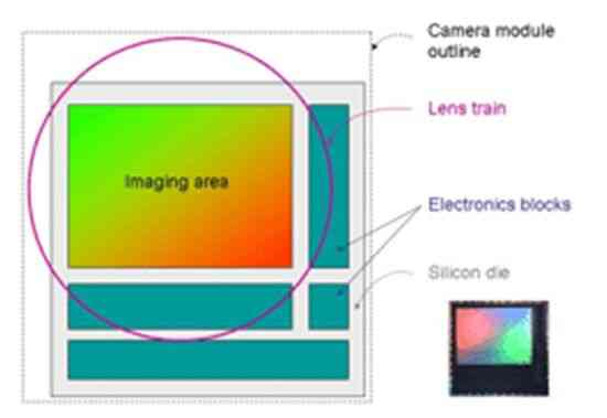
Figure 2: Image sensor chip designed to maximize wafer utilization
Since the ring-shaped optical components are concentrated in the imaging area, the effective optical area is located at a corner of the chip, and the electronic components are collectively utilized together with a larger camera module volume.
Today, from the point of view of wafer utilization, modern image sensing chip design has not been effective, but at least its imaging area is still in the center of the chip (see Figure 3). With all other factors being equal, the chip is about 8% larger than the previous generation chip, but its lens module is neatly placed on the chip, reducing the camera module by about 10% by spatial planning.
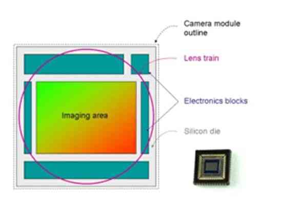
Figure 3: The imager with the detector is concentrated in the center of the chip
Although the silicon crystal of Figure 3 is physically larger than the previous generation chip, the final implemented camera module is smaller.
Reduce costs and improve reliability
The benefit of distributing the electronic block in the active imaging zone is that it forces the die pads to be distributed around the periphery of the chip. This simple change is to make CMOS image sensors compatible with wafer level packages. Wafer-level packaging has been commercialized since 2000.
Wafer-level packaging of semiconductors is cost-effective because process costs can be evenly distributed to the active chips on the wafer; on a 200mm wafer with thousands of dies, the wafer-level package cost per chip is only It takes a few cents. The wafer-level package size is determined by the chip size. Since the complete packaged chip is directly cut from the wafer, the chip size is equivalent to the package size. This feature is different from the general semiconductor packaging scheme, so wafer level packaging is sometimes referred to as 'chip scale packaging'.
The optically active area of ​​a solid-state image sensor is susceptible to mechanical and environmental damage, primarily because its surface is covered with precision optical components such as color filters and microlens arrays. The wafer level package of the image sensor can cover the front side of the wafer with a layer of glass wafer to protect these optical structures. However, this causes problems in that it cannot be connected to the pad, and the conventional wire bonding method can no longer be used.
In theory, we can also connect to the pad by means of silicon vias. However, despite the many years of efforts in TSV technology, it has not been widely adopted by the industry. The reason is that this method needs to invest some special equipment to manufacture via holes, and the reliability of TSV interconnection has not yet reached the level of industry satisfaction under the premise of cost competition.
The only wafer level packaging solution that has been used in mass production today is edge contact. As the name suggests, the portion for contact is placed on the edge of the pad, while the trace on the line provides a conduction path for the ball grid array (BGA) package. This type of contact has been proven to provide reliability and durability, while the BGA enables packaged imagers to be compatible with both retracted and wound reflow assemblies, as are the assembly of all components inside the phone. The compatibility of the pin-free surface mount assembly eliminates the need to integrate the imager into the handset's flexible circuitry and connectors. Connector failure has always been the main cause of the camera phone returning to the factory for repair. According to Prismark, in 2006, more than 225 million image sensors were built with edge-contact wafer-level packaging. In addition, the company expects that by 2011, more than 50% of CMOS imagers will use this. Packaging method.
Edge contact has a small drawback, that is, chips on the wafer must be reserved for a wider space than usual to reserve a path for architecture development. As a result, the maximum number of chips that can be realized on each wafer is reduced, and the unit cost is relatively increased. The latest generation of wafer-level packages for image sensors solves these problems with interconnect-via-pad interconnect technology. Figure 4 shows a similar case. The interconnect still uses edge contact technology but is presented in a neat radial pattern within the pad area. This not only makes the chip cutting channel narrower under the conditions allowed by the silicon crystal design rules, but also removes many pad size, pitch and position restrictions, making this wafer level packaging method directly compatible with most Existing CMOS imager.
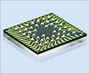
Figure 4: SHELLCASE's MVP wafer-level package contains a solid-state image sensor
The package uses vias through pad edge contact technology to provide a compact and rugged package that is compatible with pinless assembly that can be implemented in a low cost process.
Innovations in materials and processes have succeeded in reducing the thickness of packaged imagers by approximately 500 μm, making them immediately suitable for use in electronic products that are currently pursuing a trend toward thinning. This advantage directly reduces product cost, making wafer-level packaging with vias through the pad interconnects a key driver of the sacred development of the mobile phone market—developing a $1 VGA camera module.
Excellent metal material, which guarantees durability.
Processed by precision machine tool, standard G1/4 screw thread with good compatibility.
Electroplating on the surface, anti-oxidization and resistant to corrosion.
Mature sealing process, high-quality sealing components, safe, leakage-proof, and more reliable.
Pure Copper Connector,Pure Copper Wire Connector,Pure Copper Terminal Connector,Pure Copper Smc Connector
Dongyuan Syscooling Technology Co., Ltd. , https://www.syscooling.com