Wireless sensor network (Wireless Sensor Network, WSN) with its advantages of low complexity, low cost, low power consumption, many network nodes, etc., is more and more widely used in real life, especially the emergence of some system on chip (SoC) , Greatly reducing the difficulty of developing wireless sensor networks. When using these system-on-chips for the development of wireless sensor networks, because the transmission power of the wireless communication part of the system-on-chip itself is very small (such as the transmission power of CC2531 is only 4.5 dBm), plus its receiving sensitivity is also fixed at a certain level In this way, the communication distance of the wireless sensor network is limited, and the common transmission distance is several hundred meters. In some specific application environments, the placement distance between network nodes is required to be more than one kilometer or even farther.
This paper introduces a wireless sensor network node design based on the core chip CC2531. It uses TI's 2.4 GHz RF front-end chip CC2591 to increase the transmission power of the wireless communication part and further improve its reception sensitivity, thereby extending the communication distance.
1 Introduction to the core chip
1.1 CC2531
CC2531 is a system-on-chip (SoC) solution for the IEEE 802.15.1, ZigBee, and RF4CE applications with USB functions introduced by TI. It can build powerful network nodes with very low total material cost. CC2531 integrates 2.4 G. Hz RF transceiver, enhanced industry standard 8051 MCU, in-system programmable 256 KB Flash, 8 KB RAM and many other powerful functions; the transmit power is 4.5 dBm (adjustable), and the receiver ’s receiving sensitivity is -97 dBm.
1.2 CC2591
CC2591 is a RF front-end chip launched by TI that works at 2.4 GHz and is aimed at low-power and low-voltage wireless applications. CC2591's internal integrated power amplifier (PA) has a gain of 22 dB, a maximum transmit power of +22 dBm (input +5 dBm), and an output of 1 dB compression point of +19 dBm. The internal integrated LNA of the receiving part is divided into high and low receiving gains. 11 dBm, 1 dBm, the noise figure is 4.8 dB, and the receiving sensitivity is improved by 6 dB.
2 Overall design
According to the design requirements, the block diagram of the system hardware structure is shown in Figure 1. The core chip CC2531 combined with its peripheral circuits (such as crystal oscillator, A / D reference voltage, memory, sensor and debugging interface, etc.), plus the necessary power module and RF front-end chip CC2591, constitute the hardware system of this solution. When applied to different fields, the corresponding sensors, power supply, A / D reference voltage, memory, etc. can be adjusted accordingly. The hardware design of CC2531 and CC2591 is relatively fixed.
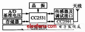
Figure 1 Block diagram of system hardware structure
3 Performance parameter budget
3.1 Transmit power budget
According to the data sheets of CC2531 and CC2591, the maximum transmit power of the CC2531RF port is +4.5 dBm, and the value of the TXPOWER register can be adjusted to adjust its transmit power, ranging from -22 to +4.5 dBm. After connecting CC2591, the maximum PA gain in CC2591 transmission mode is 22 dB, then the corresponding transmission power range is + 22 ~ 10 dBm (the maximum value is determined by the PA itself, the minimum value can be smaller). Taking into account the PA's 1 dBm compression point (19 dBm) and system power consumption and other factors, set its TX-POWER = 0xD5, that is, the output power of CC2531 is 1 dBm, and the transmit power of CC2591 is 19 dBm, which is ideal. Power output reference setting (for reference only, may change in practice).
3.2 Estimation of receiving sensitivity
When CC2591 is in receiving high gain mode, HGM = 1, the noise factor NF of its external antenna and internal T / R selector to internal LNA is 4.8 dB, and the signal-to-noise ratio SNR of the analyzable signal inside the back-end CC2531 is 3 dB (to ensure that the bit error rate is at a certain level), the single channel transmit and receive bandwidth BW can be set to 1 MHz or 5 MHz. According to the formula, when the normal room temperature T0 = 290 K, the noise power of 1 Hz bandwidth is N0 = -174 dBm, and the receiving sensitivity S = -174 dBm + NF + SNR + 10log (BW).
Substituting parameters can be obtained: when the receiving bandwidth is 5 MHz, the receiving sensitivity S = -99. 2 dBm.
3.3 Communication distance estimation
In the real environment, communication between any two points, the loss caused by the environment to the transmission wave is generally not quantitatively estimated, and varies widely according to the environment. Without considering external influences and transmission loss, under the condition that electromagnetic waves propagate under ideal conditions, the calculation formula of wireless communication transmission distance is as follows:
Loss = 32.44 + 20lgd + 201gFreq
The antenna gain is not considered for now (it needs to be determined according to the actual antenna parameters purchased). The link loss budget Loss is 118.2 dBm (excluding non-ideal loss), and the frequency Freq is calculated at the RF center frequency of CC2531 at 2450 MHz, and the wireless communication transmission distance d = 7.93 km. In practical applications, this distance cannot be reached, this value is for reference only.
Welding diodes are available for medium frequency (over 2KHz) and high frequency (over 10khz) applications.They have very low on - state voltage and thermal resistance. Welding diodes are designed for medium and high frequency welding equipment and optimized for high current rectifiers. The on-state voltage is very low and the output current is high.
Welding Diode,Disc Welding Diode,3000 Amp Welding Diode,High Current Rectifier Welding Diode
YANGZHOU POSITIONING TECH CO., LTD. , https://www.yzpst.com