introduction
This article refers to the address: http://
Since its establishment, the global positioning system (GPS) has been widely used, and has played a huge role in aerospace, military, economic, communications, electric power, transportation and other fields. The function of the timing system is to accurately synchronize the clock of the timepiece or measuring instrument with the international standard time. An atomic clock is usually used to ensure that the time of the instrument is accurately synchronized with the national standard time, but the atomic clock is expensive. Commonly used timing methods mainly include radio timing, satellite timing, and network timing. The use of navigation satellites for object positioning, clock timing and synchronous data acquisition control can achieve the accuracy of traditional measurement control methods, and can obtain local positioning information and other data. This satellite positioning timing synchronization technology is widely used in aviation navigation, land transportation, scientific investigation, polar exploration, geographic measurement, weather forecasting, equipment inspection, system monitoring and so on. The GPS clock adopts the world coordination time-UTC, and the cesium atomic clock which is synchronized with the UTC time on the GPS satellite becomes a space time reference. The user can receive the time service signal of the GPS satellite, correct the local clock, and synchronize with the GPS clock. Complete the time delivery task, called GPS timing.
2 Working principle
The GPS timing server is mainly composed of AT89S52 single-chip microcomputer, LCM display module and GPS OEM module GPS25-LVS and output module. It can display real-time information such as latitude and longitude, Beijing time, speed, etc. The system principle is shown in Figure 1.

The MCU is used as the main controller to initialize the GPS25-LVS module. The GPS25-LVS module receives the signal transmitted by the satellite, and outputs the NMEA-0183 format statement. After the solution processing by the MCU, it is sent to the LCM liquid crystal display module for display. The output module provides a second pulse (1PPS) signal with multiple electrical characteristics.
3 hardware design
3.1 GPS OEM module selection
GARMIN's GPS25-LVS series OEM board [4] uses a single 5V power supply, built-in protection battery, RS232, TTL two levels automatically output NMEA 0183 2.0 format (ASCII character type) statement, is currently the most widely used GPS receiving processing One of the boards can meet the needs of various navigation and timing areas. With high cost performance and strong market competitiveness, its main performance characteristics are as follows:
12 channels in parallel, can receive 12 satellite positioning time at the same time: recapture <2sec, hot start for 15sec, cold start for 45sec, automatic search for 90sec
Positioning accuracy: 15mRMS / differential <5m
It can receive real-time differential signals for precise positioning. The signal format is RTCM SC-104, and the baud rate is adaptive.
1PPS second pulse signal output, accuracy index up to 10-6 seconds dual serial port (TTL) output, baud rate can be set by software (1200 ~ 9600)
Sensitivity: -166Dbw
Antenna interface: 50 ohm MCX connector active antenna (5V)
3.2 Data output format of GPS25-LVS module
The default communication baud rate of GPS25-LVS is 4800, 1 start bit, 8 data bits, 1 stop bit, no parity. It is usually output in NMEA-0183 format, and the data code is ASCII characters. NMEA-0183 is a standard format developed by the Ocean Electronics Association of the United States for marine electronic devices. V2.0 is widely used. Since the format is an ASCII code string, it is intuitive and easy to process. In many high-level languages, it can be directly discriminated and separated to extract the data required by the user. The GPS25-LVS series OEM board can output 12 sentences, namely GPGGA, GPGSA, GPGSV, GPRMC, GPVTG, LCGLL, LCVTG, PGRME, PGRMF, PGRMT, PGRMV, GPGLL.
3.3 GPS OEM connection with AT89S52
The GPS25-LVS OEM board has two serial ports, and its serial port 2 is used to receive GPS differential information and phase data output of RTCMSC2104 version 2.1. Serial port 1 is an asynchronous serial data communication interface, so asynchronous serial data communication with the AT89S52 microcontroller is possible. Since the level of the serial port configuration is the standard RS-232 level, and the output voltage of the AT89S52 MCU is 0 to 5V TTL level, the voltage specifications of the two are inconsistent, so the communication cannot be directly performed. To make the TTL level and RS The -232 standard is compatible with MAXIM's multi-channel transmission and receiving integrated chip MAX232 to realize serial communication between the microcontroller and the OEM board. The second pulse signal is also output after the GPS25-LVS OEM board is initialized. The 1pps signal is processed by the CPLD as an external interrupt source of the microcontroller to synchronize the time information, and is also used to monitor whether the signal is normal.
3.4 Matrix keyboard and LCM display
Design a 2×4 matrix keyboard that responds to user actions while the system is running. The buttons have functions such as “Menuâ€, “Upâ€, “Down†and “Clearâ€. During the operation of the single-chip computer program, the key operation is detected in real time. When a button is pressed, the operation of debounce, scan, etc. is performed, the key value of the key is obtained, and different codes are executed according to the key value and the current state to implement keyboard multiplexing.
In the system, the HTM4002A dot matrix graphic liquid crystal module is used. The module uses S6A0069 to control the driver. It has a built-in national standard one or two-level font library. The liquid crystal module not only displays characters and Chinese characters, but also displays continuous and complete graphics. The module is powered from a single supply of 5V and requires no negative pressure.
3.5 logic circuit and output
The logic circuit is mainly implemented by CPLD. It uses Altera's MAX 7000S series EPM-7128. The MAX7000 products based on electrically erasable programmable read-only memory (EEPROM) are manufactured in an advanced CMOS process, providing 32 to 512 macros. The cell's density range, from pin-to-pin delay of 3.5 ns. Support for System Programmability (ISP), which can be easily reconfigured in the field.
The EPM-7128 generates a local second pulse that does not function when there is a GPS second pulse. Instead of GPS, it provides a second pulse output to the microcontroller when the GPS signal is lost. As shown in Fig. 2, the signal 1 is the local second pulse, which is obtained according to the rising edge of the 1PSS signal of the first 1S as the starting time, and the timing is 1S, and the self-generated pulse is not covered normally in a certain error condition. The GPS second pulse at work, so a delay Δt is added, and when the GPS signal is detected, Δt is removed to replace the GPS second pulse. Signal 2 is a narrow pulse signal output from EPM-7128, which is used to shield the pulse interference. It is distributed on both sides of the rising edge of the GPS second pulse and is operated with the GPS second pulse. Impulse interference outside the narrow pulse is masked. This achieves the function of preventing GPS signal failure and anti-interference pulse.

The output modules include MAX232, DS90C031, 74HC245 and other chips, which convert the output of the EPM-7128 into a second pulse signal output of various electrical characteristics such as 232, differential and TTL, providing a convenient solution for various applications.
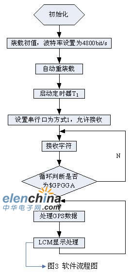
4 software design
The system is implemented by C51 programming [2]. The main program flow is shown in Figure 3. First, the data output by the OEM board is output in the form of data stream. The starting time of the acquisition is not necessarily the start time of one frame of data, so the data is in the data. When collecting, you must first determine the header block, and after receiving the header block, start collecting data. Set the baud rate of the MCU to 4800 bit/s, which is consistent with the transmission baud rate of the GPS OEM board. Send an instruction to the OEM board to send the 0183 data format as “$GPGGAâ€. The instruction is pre-existing in the data memory, and the data is sequentially retrieved from the program memory in a cyclic manner, and then the OEM board outputs the corresponding Formatted data. The MCU judges the received information. Since the received time is Coordinated Universal Time (UTC), it is accurate Beijing time to add 8 hours to this time, and the time information is processed accordingly, and then displayed.
5 Conclusion
The GPS OEM board's serial output is coordinated by the world time. It is easy to operate, practical, and provides a rich second pulse interface to meet the requirements of most users. When the GPS signal is normal, it has high precision, and the timing system is tested in the laboratory with an error of less than 100 ns. The result is satisfactory. The accuracy is also guaranteed when the GPS signal fails, but its accuracy and stability are directly related to the frequency accuracy and stability of the constant temperature crystal. If the CPLD uses a higher precision clock signal, the result will be more ideal.
Copper Conductor Power Cable,Copper Conductor Insulated Cable,Copper Conductor XLPE Cable,12KV Copper Conductor Cable
Huayuan Gaoke Cable Co.,Ltd. , http://www.bjhygkcable.com