The rapid development of wireless communication and network technology has provided conditions for information exchange anytime and anywhere, which has made great changes in the intelligent transmitter as an important part of the remote monitoring system. In the past, the complicated and complicated connection was gradually improved by high efficiency and automation. The communication method is replaced. The smart transmitter with wireless communication and network functions is easy to deploy, as long as it is in the area covered by the network, the communication function can be completed, and it is not easy to be affected by the target environment. It is especially suitable for being placed in an unattended place in military defense. Industrial and agricultural, urban management, biomedical, environmental monitoring, disaster relief, anti-terrorism and anti-terrorism, remote control of hazardous areas and many other fields have great practical value and broad market prospects.
The overall design of the intelligent wireless signal transmitter
Smart wireless signal transmitters are designed for mainstream transmitters and typical sensor output signals, so first analyze their respective output signals. Usually the output of the transmitter is a 4 to 20 mA standard current signal. For sensors, there are many types of output signals. In view of the object of the system design, the non-electrical signal and the large voltage signal which are less targeted for professional applications are not considered. In addition, for the more commonly used frequency signals, there is no consideration when designing the system prototype. This can be added in the development of the product prototype to increase the flexibility of the system. Comprehensive analysis, the focus is on the weak voltage signal. So how do you determine the range of weak voltage signals that the system is designed for? In general, the mV-level voltage signal is considered to be a weak voltage signal, but the concept is vague and not easy to quantify. Depending on the extent of the application, the representativeness, and the extent of the specification, it is possible to analyze the thermocouple as an example.

Figure 1 system principle framework
The thermocouple generates a voltage (potential) signal, which is a slowly varying millivolt-level weak signal. Table 1 shows the temperature measurement range and corresponding thermoelectric potential range of various commonly used thermocouples.
Table 1 Main technical parameters of commonly used thermocouples
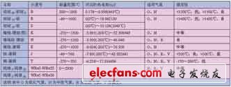
It can be seen from the table that the output thermoelectric potential of the thermocouple is basically in the range of 0 to 60 mV. Therefore, it can be considered that 0 to 60 mV is well represented, can cover many application environments, and should also be input as a system. Another type of signal. There are two types of input signals at the front end of the system: 4 to 20 mA standard current signals and 0 to 60 mV voltage signals. These two types of signals are conditioned by different conditioning circuits to be suitable for the voltage signal of the A/D chip input range, and then subjected to analog-to-digital conversion through multi-switch gating, and then processed by the MCU, and finally can communicate with other field devices or monitoring centers. . The system principle framework is shown in Figure 1.
hardware design
The following describes the design of the hardware circuit from the aspects of signal conditioning circuit, AD conversion circuit and GPRS MODEM interface circuit.
1 signal conditioning circuit
The function of the signal conditioning circuit is to amplify the two input signals of the 4-20 mA standard current signal and the 0-60 mV voltage signal, and realize the strobe input through the multiplexer for the subsequent AD conversion.
Since the dynamic range of the input signal of the system design is 0-60mV, the value is smaller than the input range of common A/D chip (2V, 5V, ±10V, etc.). If it is directly converted, it will not be possible. The conversion accuracy affects the overall measurement accuracy of the system. Therefore, the input signal needs to be amplified first. After comprehensive consideration, the instrument operational amplifier INA118 is used.
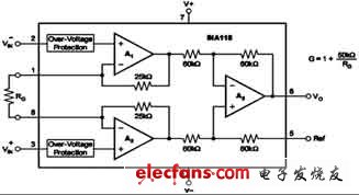
Figure 2 INA118 internal circuit diagram
The INA118 achieves different gains by connecting resistors Rg between pins 1-8, which can vary from 1 to 1000. The magnitude of the resistor Rg is determined by Rg = 50 kΩ / (G - 1), where: G is the gain.
Since the stability of Rg and the temperature drift have an effect on the gain, the requirement for Rg is also high in applications requiring high-accuracy gain, and high-precision, low-noise metal film resistors should be used. In addition, the Rg value in a high gain circuit design is small, such as an Rg value of 1.02 kΩ at G=100 and an Rg value of 50.5 Ω at G=1000. Therefore, the wiring resistance at high gain cannot be ignored, and the actual gain may have a large deviation due to its existence, and thus the calculated Rg value needs to be corrected. The specific method of correction is to replace Rg with an adjustable potentiometer, and adjust the potentiometer so that the ratio of the output voltage to the input voltage reaches the gain value required by the design.
The 4~20mA current signal can be converted to voltage signals of different dynamic ranges by using different resistance sampling resistors. According to the requirements of this system, a 120Ω precision resistor can be used to convert a 4-20mA current signal into a voltage signal of 0.48~2.4V, which is matched with the downstream A/D chip range. The signal conditioning circuit is shown in Figure 3.
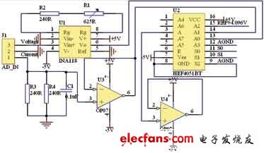
Figure 3 signal conditioning circuit
Extra High Voltage Electric Pole
Extra High Voltage Electric Pole,Utility Pole Lights,25Ft Power Pole,Hot Dip Steel Wire Pole
JIANGSU HONGGUANG STEEL POLE CO., LTD. , https://www.hgsteelpole.com