Microprocessors and application-specific integrated circuits (ASICs) demand power supplies that operate at low voltages but high currents. These power supplies must maintain tight control over output voltage, especially during load transients. This makes testing and verifying compliance with specifications a complex and challenging task for designers.
This article explores key questions about load transient testing and provides practical solutions to simplify the process under demanding conditions.
To design an effective power supply, it's essential to understand all the transient parameters involved in testing. Common parameters include:
- The magnitude of the load step (in amps or as a percentage of full load)
- The minimum load during transients (which may be zero)
- The rate of the load change (typically in amps per microsecond)
- The maximum allowable voltage deviation
- The estimated recovery time after the transient
Figure 1 shows how these specifications are typically defined.

Figure 1: Graphical representation of load transient measurements.
Once you have a clear understanding of these parameters, you can begin designing a power supply that meets your needs. However, testing according to these strict requirements presents significant challenges. For instance, a 1V output with a 100A load step and a 1000A/μs slew rate is not typical. In most cases, the limiting factor is the parasitic inductance between the power supply and the load. In real-world systems, the power supply is usually placed close to the load to minimize this inductance.
There are several methods for testing the load transient response of a power supply, each with its own advantages and drawbacks. In this article, we’ll compare the following options: external electronic loads, external transient boards, FET slammers, onboard transient generators, and socket-based transient testers.
External electronic loads are the most commonly used and convenient method for transient testing. Most models allow users to easily set current levels and transition times. However, they often suffer from limitations due to external wiring or load capabilities, which can restrict the achievable slew rate.
External transient boards offer better performance in terms of slew rate but come with reduced flexibility. Depending on the design, they may be limited by maximum current, heat dissipation, or board layout. Since they are external, wiring can still be a bottleneck, and each test may require reconfiguration of the board.
FET slammers provide a fast and simple way to achieve high-speed transients. A metal-oxide semiconductor field-effect transistor (MOSFET) is connected from drain to source via a resistor or directly to the power supply output, with the gate controlled by a function generator. The minimal external wiring reduces parasitic inductance significantly.
While FET slammers can produce high slew rates, they can be difficult to control and repeat. They may also require modifications to the PCB (see Figure 2). Another issue is the difficulty in accurately measuring the actual load step current, which can lead to unreliable data.
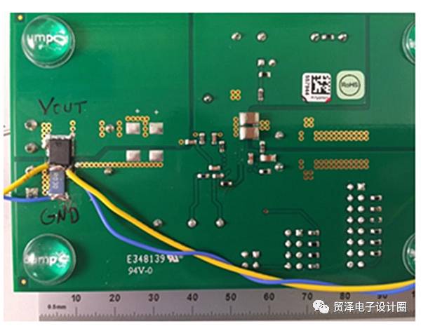
Figure 2: Example of a PCB modified for an FET slammer.
For high-current, high-speed transient testing, an onboard transient generator is a practical solution that can be tailored to specific load transient requirements. However, it adds cost and space to the design. Moreover, taking multiple measurements can be time-consuming or complicated.
The design of an onboard transient generator can vary widely, from a simple setup using a 555 timer and FET to more advanced configurations like the one shown in Figure 3. A complex design may use multi-stage switching FETs to achieve a slew rate of up to 1000A/μs.
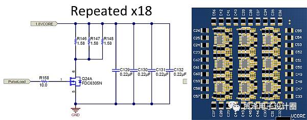
Figure 3: Advanced onboard transient generator design.
The final option is to use a processor socket along with a dedicated transient tester. While this method is the most expensive—due to both the tool itself and increased PCB costs—it offers the highest accuracy for specific processor or ASIC requirements. Many manufacturers develop such tools to ensure precise test conditions.
Table 1 summarizes the different transient testing methods discussed above.
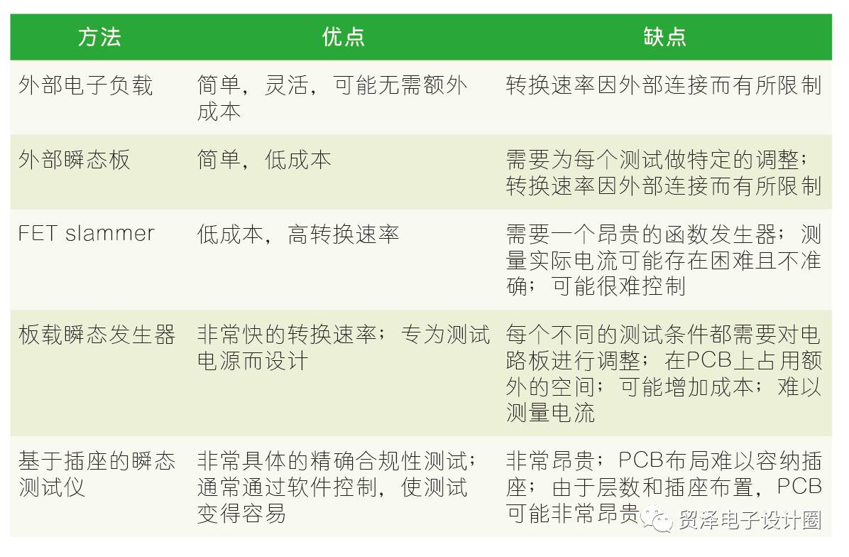
Table 1: Comparison of various transient test methods.
Load transient testing is a critical part of power supply design and validation. Parasitic inductance in the test setup can severely limit the ability to achieve the desired slew rate. By using the methods outlined here, engineers can overcome these challenges and improve the accuracy and reliability of their tests.
Deep Cycle GEL VRLA Batteries,deep cycle battery,gel battery,valve regulated lead acid vrla,valve regulated lead acid,golf buggy batteries
EMoreShare International Trade (Suzhou) Co., Ltd , https://www.emoreshare.com