DBPL (Differental Bi-Phase Level) coding is a coding method that exceeds the limits of traditional digital transmission. DBPL coding is widely used in engineering applications such as Ethernet, engineering logging tools and railway transponders. In railway transponders, DBPL coded transmission signals are sent to the train's on-board processor to control train operation.
This text has designed a kind of signal source system of DBPL coded signal based on AT89LV51 one-chip computer control, can produce DBPL coded signal; At the same time design the systematic power management module, guarantee the normal power supply of the system.
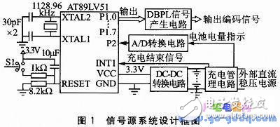
1 Design of signal source systemThe signal source consists of a clock reset module, a DBPL signal generation circuit, a DC-DC conversion circuit, a charge management circuit, and an A/D conversion circuit. MCU AT89LV51 control coding module generates DBPL signal; charge management circuit to charge the battery used by the system to ensure that the battery is fully charged; DC-DC conversion circuit for the microcontroller and the logic to generate a stable voltage supply; A / D conversion circuit to collect battery power Information, and inform microcontroller processing. The signal source system design block diagram is shown as in Fig. 1.
1.1 DBPL signal generation circuit
In this design, the DBPL signal is synthesized from a sine wave as an energy carrier and a pulse coded signal. The pulse coded signal is coded by DBPL. The average transmission rate is 564.48 kb/s. The energy carrier is a sine wave and the signal frequency is 8.82 kHz. The input of the module is 8-bit parallel binary data to be encoded. It is connected to the P1.0-P1.7 of the AT89LV51 microcontroller and controlled by the microcontroller to provide input. DBPL signal generation circuit schematic shown in Figure 2.
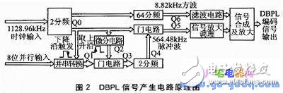
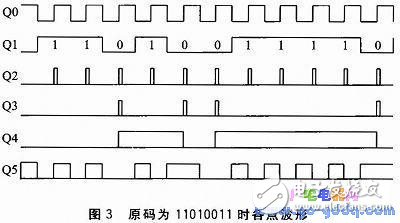
Among them, the parallel to the serial circuit uses an 8-bit parallel-to-serial conversion shift register 74166 and a slice counter 74163. The counter 74163 uses the modulo 8 count. When the counter reaches 8 counts, the counter is cleared to restart counting; during counting, 8-bit parallel data is output according to the clock beat. Two frequency dividers and 64 frequency dividers are implemented using the counter 74163. Differential circuit using D flip-flops and gate circuits to achieve. The parallel-to-serial conversion output Q1 is summed with the rising edge Q2 obtained by the non-gate and the differential circuit to obtain Q3. The D flip-flop is used to realize a 2-frequency output Q4. Finally, the Q0 and Q4 are exclusive-ORed to obtain the encoded output. Output 8.82kHz square wave and 564.48 kHz pulse wave, and then filter, amplify conditioning, and then synthesis into the final DBPL signal. Assume that the single-chip input parallel data is 11010011, and the waveforms of each point in Figure 2 are shown in Figure 3.
1.2 Charge Management Circuit
Considering the portable system, the system uses a rechargeable battery (six nickel-metal hydride batteries) to supply power to the system. The voltage of each battery is 1.2 V. At the same time, the battery management chip MAX713CPE for the nickel-metal hydride battery is used. Management is performed to ensure that the battery is safe and fully charged, and the power supply module is controlled and detected by the microcontroller.
The MAX713CPE is a fast charge management chip for NiMH and NiCd batteries. It has the following features:
â—† The number of batteries, charging time and current size can be adjusted;
â—† zero voltage slope detection, fast, trickle charge the battery;
◆ When the battery is not charging, the maximum current consumption of the chip is only 5μA;
â—† Less external circuits are needed, and only one PNP pin is required to achieve basic charge management.
Charge management circuit shown in Figure 4. The VLIM pin is used to set the maximum battery voltage. It has the following relationship with the battery voltage and the number of battery cells:
(BATT+-BATT-)≤(VLIMIT&TImes;n)
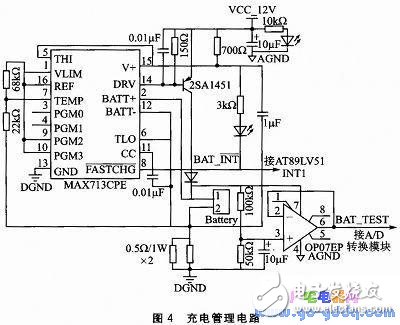
Among them, (BATTC+-BATT-) is the voltage across the battery, n is the number of cells, under normal circumstances VLIMIT can be connected to the REF pin. The PGM0 and PGM1 pins are used to set the number of sections to be charged (1 to 16 sections): PGM0, PGM1 can be selectively connected to any of the V+, REF, BATT- pins or left floating as required. The rechargeable battery is set to 6 knots. The PGM2 and PGM3 pins are used to set the maximum fast charge time. According to the same method as setting the PGM0 and PGM1 pins, the maximum fast charge time (33 to 264 min) can be set as required. In this design, it is set to 120 minutes.
This system also realizes the detection of the battery power. In Fig. 4, the voltage of the battery is detected by the amplifier OP07EP and sent to the A/D conversion circuit. Finally, it is submitted to the single-chip microcomputer for processing.
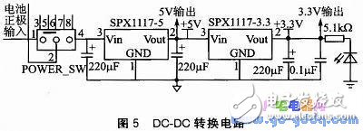
The battery voltage output is 7.2 V, which can reach 7.4 to 7.6 V in full charge. The voltage used by the microcontroller is 3.3 V, and the voltage required by the DBPL signal generation circuit is 5 V. This requires a DC-DC converter circuit to convert the rated voltage of 7.2 V to 5 V and 3.3 V. Two-stage conversion is used: the first stage converts 7.2 V into 5 V to supply the DBPL signal generation circuit, and the second stage converts 5 V into 3.3 V to supply the microcontroller. The system uses SPX1117 (SPX1117-5 and SPX1117-3.3) as the regulator chip in the DC-DC conversion circuit. The chip is characterized by a low dropout voltage, with a voltage drop of only 1.1V at 0.8A and an optional voltage (5V and 3.3V). DC-DC conversion circuit shown in Figure 5.
After the system design was completed, a detailed test experiment was conducted. The test results show that the input signal can be well controlled by the programming of the SCM. The sine wave amplitude and pulse wave amplitude of the signal source output meet the application requirements and can be widely used in the field of simulation test and project experiment. If you need further amplification, external amplifier circuit and external power supply must be connected. The DBPL coded signal transmission rate is the specified 564.48 kb/s. The power management circuit can effectively manage the battery, and the charging time is maintained at approximately 120 to 140 minutes. After the battery is full, trickle charging is performed. During use, the microcontroller can monitor the battery power and alarm in real time through the A/D converter circuit. The voltage output from the DC-DC converter circuit is stable and the power consumption is low.
Rotary encoders are used as sensors for angle,position,speed and acceleration. We can offer incremental encoders and absolute encoders.

Absolute Encoder,Custom Encoder On Motor,Custom Optical Encoders,High Resolution Encoder
Yuheng Optics Co., Ltd.(Changchun) , https://www.yhenoptics.com