With the rapid development of 3G network technology and the enhancement of various functions of 3G mobile phones, it has become possible to use 3G mobile phones to realize video surveillance anytime and anywhere. Embedded technology, as a popular technology in today's IT industry, various embedded chips such as DSP, ARM, SOC, etc. are widely used in digital, security, traffic signal acquisition, telemedicine and other fields, can predict the future of portable multi-functional personal medical Digital service terminals will be as popular as mobile phones, and users can transmit their important physiological information to remote medical centers or home care experts in real time, accurately, and quickly anytime, anywhere, so as to obtain professional advice and guidance from doctors to achieve remote medical monitoring. Applications. This paper designs a 3G mobile phone embedded video acquisition system based on ARM9 chip. Compared with the general video acquisition system, this system has the characteristics of small size, low energy consumption, convenient update and maintenance, and low development difficulty.
1 System hardware structure
The hardware platform of this system is shown in Figure 1. In view of the reliability, scalability and maintainability of the system, this system adopts a modular design principle. The hardware of the video acquisition system of the entire system is composed of 3 parts.
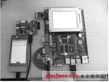
Figure 1 physical hardware platform
1. 1 Microsystem core module
The module is composed of embedded microprocessor S3C2440A, NANDFALSH interface circuit, SDRAM interface circuit and bus interface circuit. S3C2440 is Samsung's 32-bit RISC microprocessor chip based on the ARM920T core, providing a low-cost, low-power, high-performance small microcontroller solution for handheld devices and general types of applications. A new bus architecture AMBA is adopted, and its core also implements MMU, Har vard cache architecture. In addition, its enhanced ARM architecture MMU supports WinCE, Linux, EPOC32 and other operating systems [9], supports ARM modulation architecture, and supports booting from NAND FLA SH memory. Moreover, it also integrates rich on-chip functions, such as LCD controller, UART interface, USB master-slave interface, I2C interface, CAM IF unit, etc.
Although SDRAM can't save data when power off, it has very high read and write speed, so it is suitable for the main program. This system uses two 32 MB HY57V561620 chip cascades to form a 64 MB SDRAM memory. The internal storage structure of the chip is 4 Banks & TImes; 4M & TImes; 16 b, a total of 4 banks. The NAND FLASH storage system uses the K9F1208U0M chip from Samsung with a storage capacity of 64M & TImes; 8b. The interface connection between the core module and the peripheral control module is realized by the bus interface.
1. 2 video capture module
The module uses the CMOS camera interface of the Micro2440 development board, and directly uses the CAM130 camera module provided by the friendly arm. The module is composed of a 1.3-megapixel CMOS image sensor OV9650 and its interface circuit and power circuit. CMOS sensor is selected because it has the advantages of high integration, small size, low power consumption, convenient programming, easy control, low cost, etc., and this type of sensor is developing in the direction of low noise and high sensitivity, so CMOS sensor is the current The best choice for low-pixel image acquisition systems. The interface circuit performs A / D conversion and processing on the image signal and transmits it to the CAM IF of the processor.
The core module of the micro system realizes the control of the sensor through the I2C serial bus. The power supply circuit is provided with 1. 8 V and 2. 8 V voltages for the camera by the power conversion chip A S1117, where the 2.8 V voltage is obtained by dividing the voltage of the adjustable voltage chip (that is, VDD_CAM in FIG. 2). The power supply voltage of the module is 3.3 V, which is the same as the power supply voltage of the core module of the microsystem, and does not need to be provided separately.
1. 3 Peripheral Control Module
The module is composed of LCD and touch screen interface circuit, JTA G debug interface circuit, U SB master-slave port circuit, reset circuit, power circuit, RS 232 serial port circuit, etc. The LCD and touch screen interface circuit is used to display the video data collected after the application program is written and to accept the user's external control commands. The JAT G debugging interface provides the function of hardware debugging. It follows the IEEE 11491 standard and uses boundary scan technology to realize the observation and control of the chip input and output signals through the boundary scan chain. An important function of JATG in this system is to burn the boot loader Boot loader into the development board for further kernel loading. The USB main port is used for external U disk, mobile hard disk, mouse and other devices that support U SB bus interface, which can expand the storage space.
The USB slave port is used to program the WinCE kernel file to the system and the communication between the system and the PC. The reset circuit uses a special reset chip MAX811 that has both power monitoring and data protection and a watchdog function to ensure that the system can be reliably reset when an abnormality occurs. RS 232 is used to view the boot loader program startup status and extended serial communication function through Hyper Terminal or DNW tool. The power supply circuit here provides 5 V (providing external power for the entire system), 3.3 V (core module, peripheral control, image acquisition module power supply) and 1.3 V (core module power supply).
Compabile Models:
For Samsung:
For Galaxy S6, For Galaxy S6 Edge, For Galaxy S6 Edge+,
For Galaxy S6 Active, For Galaxy S6 Duos, For Galaxy Note Edge,
For Galaxy S7, For Galaxy S7 Edge, For Galaxy Note 5
For Galaxy S8, For Galaxy S8 Plus, For Galaxy Note 8
For Galaxy S9,For Galaxy S9 Plus
For Sony:
For Xperia Z4V, For Xperia Z3V
For Google:
For Nexus 4, For Nexus 5, For Nexus 6, For Nexus 7
For MOTORALA:
For Moto Droid Turbo, For Moto Droid Turbo 2, For Moto Droid 5
For NOKIA:
For Lumia 920, For Lumia 928, For Nokia Lumia 93, For Lumia 950, For Lumia 950 XL, For Lumia 1020, For Nokia Lumia 1050, For Nokia Lumia 822, For Nokia Lumia 735
For HTC:
For HTC ONE MAX T6, For HTC Incredible 4G, For HTC ONE mini 2, For HTC Droid DNA
For LG:
For LG Nexus 4, For LG Nexus 5, For LG G Pro, For LG D1L, For LG LTE2
For Iphone:
For Iphone8/X/XR/XS Max
For Others:
For YotaPhone 2, For Elephone P9000
Guangzhou HangDeng Tech Co. Ltd , https://www.hangdengtech.com