1 Introduction
Information collection mainly includes the collection, storage, processing and control of signals and data. It first collects and records the physical analog quantities such as temperature, pressure, flow, displacement, angle, voltage and other measured objects, and converts them into digital quantities, and then further transforms, stores, processes, records and collects. The multi-channel signal transmission methods include frequency division system, code division system, and time division system. Among them, the time division telemetry is to distinguish the telemetry signals in different time intervals. The method of using the sampled pulse amplitude to reflect the measured parameter is called pulse amplitude modulation (PAM); the method of using the sampled pulse width or position to reflect the measured parameter is called pulse width parameter (PDM) or pulse position modulation (PPM)? A set of coded pulses to reflect the measured parameters is called pulse code modulation (PCM). At present, in missile and spacecraft telemetry, PCM is the most used, followed by PAM.
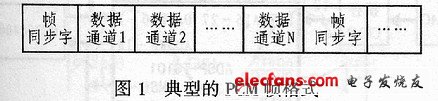
The PCM telemetry system is a commonly used telemetry device. It can collect multiple channels of data and perform communication transmission and data processing. The multiple channel data acquisition device is the editor. The editor is mainly used to control the timing of collecting the data of each data channel, and add a frame synchronization code to form a certain format of data, and then perform parallel / serial conversion to form a serial data stream and send it to the modulation device for transmission. Figure 1 is a schematic diagram of a typical PCM frame format.
2 Hardware implementation of information collection system
2.1 The principle of information collection system
The structure of the basic information collection system is shown in Figure 2. The core component is the frame format former (there are two types of ROM and CPU). On the one hand, the former sends acquisition commands and address codes to each part in time sequence, on the other hand, it collects various data and adds synchronization code groups and other information Code group, thereby forming a data frame format that is convenient for transmission. This design uses DSP to realize its function directly.

The multi-channel analog gate (commonly known as the switch) in Figure 2 uses two 16-by-1 ADG426 chips for combined design to form a multi-channel transmission gate that meets the requirements. The address code sent by the frame formatter is used as a switch control signal. The pre-amplifier circuit uses a low-noise amplifier to ensure the system's distortion-free amplification measurement of weak signals. The role of the amplifier is to provide a high input impedance for the input terminal to minimize the parameter error, and at the same time provide sufficient amplification for the signal, so that the maximum value of the measured signal reaches the A / D full scale level. Since the input level of the analog signal is specified as 0 to 5V, when measuring the AC signal, the center value should be raised by + 2.5V. The AD9240 can easily meet its requirements.
Multi-channel digital parameters wait in the interface first, and then insert the external digital quantity into the data frame format synchronously when the corresponding sampling time slot arrives. The synchronization of the time-division telemetry signal and the time slot relationship are very strict. Once the code rate and frame format are determined according to the transmitted signal and the usage requirements, all time slot formats and synchronization relationships are fixed. For the entire block of data (not a detachable word) with an external synchronization flag, the PCM frame format can be received with a window. The "stacking" of foreign data blocks in the position of the main PCM frame format window is called asynchronous embedded format. During execution, the receiving end first finds the window position according to the main PCM synchronization mark, and then the composition rule of the data block is obtained from the group synchronization mark code group of the external data. Obviously, a PCM full frame can open multiple windows. The playback data of the data recorder can be embedded in the PCM frame format for transmission in this asynchronous format.
2.2 Device selection
The ADG426 is a monolithic CMOS analog selector with sixteen inputs and a common output, which can be used as an analog switching gate in the system. You can decide which way to choose by using 4-bit binary address codes A0, A1, A2, and A3. ADG426 has chip level (monolithic level) address and control valve, it is easy to interface with microprocessor.
ADG426 adopts enhanced LC2MOS process, which has the characteristics of low power consumption, high switching speed and low impedance. Low power consumption is very practical for battery-powered systems. When in the on state, each channel can conduct data in both directions equally, and there is an input signal that exceeds the range of the power supply. When in the open state, signal levels above the power supply range will be blocked. When the channel is changed, all channels are turned off immediately before the channel is changed. In the design, when the transition is a digital input, its inherent characteristics are injected by the low charge of the minimum transient state.
The A / D converter selects a 14-bit AD9240 with a sampling rate of 10 MSPS. The AD9240 has a high-performance low-noise sample-and-hold amplifier and a programmable voltage reference. At the same time, the external reference voltage can also be selected to meet the needs of DC accuracy and temperature drift in use. The device uses a multi-stage differential pipeline structure and has digital output error correction logic, so it can ensure no missing codes in the entire temperature range. The input of AD9240 has high flexibility? It can provide a convenient interface for image, communication, medical and digital acquisition systems. Its real-time differential input structure can provide single-ended input and differential input interface. Sample-and-hold amplifiers? SHA is also applicable to multiplexed systems, which can convert full-scale levels in continuous channels, and even sample signals with a single channel input frequency exceeding the Nyquist rate. AD9240 in differential input mode, its SHA can achieve excellent dynamic characteristics, and can exceed the rated 5MHz Nyquist frequency. A single clock input is used to control all internal conversion cycles. Data output adopts direct binary output format. When the conversion range is exceeded, the OTR signal can be used to indicate overflow, and the signal can also determine whether the result is high or low.
The conversion clock of AD9240 is 5MHz, and only one valid data is taken for every 4 conversions, so 1.25MHz clock can be used as DMAR. By reading the valid data of the second conversion in the first four cycles through the DMAR signal, the influence of the 120ns switching time of the ADG426 selector can be avoided.
The AD9240 converter has a 2.5V reference voltage, and the signal can be input into the AD9240 using single-ended direct coupling. Data latching is done by CPLD. The latch clock has the same cycle as the DMAR of the DSP, that is to say: after the CPLD is latched, it can be input to the DSP through the DMA mode immediately.
TIgerSHARC DSP chip ADSP-TS101 is a high-performance static superscalar processor, optimized for large signal processing tasks and communication structures. The processor combines a very wide storage bandwidth and dual arithmetic modules, thus establishing a new standard for digital signal processor performance. Its main properties are:
â— The instruction execution speed is 300MHz, and the instruction cycle is 3.3ns.
â— There is 6M SRAM in the chip, which is divided into three modules. Each module is connected through a separate address bus and data bus, so it can be accessed at the same time. There are dual arithmetic modules in the core, each arithmetic module contains an ALU, a multiplier, a shifter and a register bank. There is a double integer ALU in the core, which can provide data addressing and pointer operation functions.
â— The I / O part contains 14 DMA channels, 4 link ports and SDRAM controller, etc. The on-chip arbitration system can also form a multi-processor system with 8 TIger SHARC DSP shared buses seamlessly connected.
ADSP-TS101 has three independent address buses and data buses. The internal data bus width is expanded to 128 bits, and the external data bus width can be expanded to 64 bits.
The comprehensive processing capability of ADSP-TS101 is excellent. Its peak computing capability can reach 1600M Flops / s, 1024-point complex FFT only needs 32.78μs, and the data transmission rate of the external bus can reach 800Mbytes / s. The data transmission rate of each link port is 250 Mbytes / s.
2.3 Timing relationship and some hardware circuits
When latched by the rising edge of the clock, its timing relationship is shown in Figure 3. Figure 4 shows a schematic diagram of part of the hardware of the system. The EPM7128 in Altera's CPLD series was also used in the design.

Figure 4 Functional block diagram
  
- Protect your battery to the back case of iPhone
-
This is wholesale price order above 200pcs each item.
-
This is replacement battery tape comes with adhesive, its stripe is used to remove battery when you disassemble iPhone.
iPhone Battery Glue Adhesive,Battery Glue Adhesive,iPhone Tape Stripe
Shenzhen Aokal Technology Co., Ltd. , https://www.aokal.com