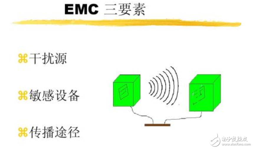
Engineers familiar with electromagnetic compatibility design all know that designing a good clock circuit is the key to ensuring that the system's radiation specifications are achieved. The EMC design of the clock circuit directly affects the performance of the entire system. For experienced engineers, there are many ways to solve electromagnetic interference problems in digital systems.
We all know that clock sources can generate electromagnetic interference in two ways. The repetitive nature of synchronous clocks and lines that are not properly terminated can generate electromagnetic interference. The energy of the clock is radiated into the electromagnetic field through the antenna. Antennas here refer to various forms: PCB lines, PCB rework lines, unshielded components, connectors, cables (shielded or unshielded), and devices that are not properly grounded. In high-speed digital systems, a fixed-frequency clock is the main source of electromagnetic interference. This is because these clocks always operate at a fixed frequency, which will increase the energy to a higher level. Non-repetitive signals or asynchronous signals do not generate so much electromagnetic interference. As higher data rates require faster clock frequencies, the signal's edge rate (ie, rise and fall times) increases. A faster edge rate will increase the energy level of the radiation signal more. The second cause of electromagnetic interference is that the clock lines are not properly terminated. Impedance mismatch will result in a positive or negative overshoot of the line signal. In this case, the radiated energy will increase. The increase depends on the severity of the positive and negative overshoot. If a serious overshoot results in ten to twenty nodes, it may not be possible to pass the FCC compliance test.
For experienced engineers, there are many ways to solve electromagnetic interference problems in digital systems. Designers can choose to shield the design, signal filtering or eliminate the interference source energy to solve the problem, these programs can be used alone, can also be used in conjunction with other programs. The first method is shielding. This is not an electrical solution. It can only be regarded as a mechanical implementation. Shielding is the use of metal packaging to surround components, circuits, assemblies, cables, or the entire system's interference sources, to prevent the electromagnetic field from spreading out. In the past, shielding schemes were often used, but sometimes the cost of such schemes was high. Moreover, for circuit systems with a relatively large amount of heat, adding a shielding box would affect heat dissipation. Without good heat dissipation, this would be very fatal for the product, and even overheating. Can damage the device or system. Also, once the electromagnetic interference problem is discovered before the product is released, if the shielding scheme is adopted, the installation of the shielding box will become a problem. The other two methods for filtering and reducing power are methods that isolate lines that generate electromagnetic interference radiation. In order to determine which one or several lines lead to electromagnetic interference, an anechoic chamber test or electromagnetic interference simulation should be performed. The test radiation reports will determine at what frequencies electromagnetic interference is exceeded, and these frequencies are often referred to as interference points. Once these frequencies (and their harmonic frequencies) have been determined, the clock lines causing the interference can be found, which can be considered from whether the clock signal is terminated, the choice of clock driver, the selection of the clock driver, or the reduction of the clock edge conversion rate.
Therefore, for the EMC design of the clock circuit, we propose the following recommendations. Since there are many electromagnetic wave interference prevention and control solutions with mechanical structures or changing circuit layouts, these solutions are time-consuming and costly. If we can pay attention to the small details of circuit design, we can effectively prevent electromagnetic wave noise. produce. If the clock signal is not properly terminated, or the clock device has fast transient characteristics, it will generate a lot of electromagnetic noise. To control the generation of electromagnetic wave noise, the following principles must be considered: correct termination of all clock signals; try to use clock buffers with lower edge rise rates; use filter capacitors in the clock lines; use in high-speed circuits Clock spread spectrum technology.
In addition to the above methods, we can also use some measures to reduce the electromagnetic radiation of the clock circuit and the clock line. For example, the length of the clock signal trace should be as short as possible, the line width should be as large as possible, and the distance from other lines should be as large as possible. Placement and routing of the device, if necessary, can go to the inner layer; clock generator as close as possible to the device that uses the clock. In some cases, a protective line may be added to the clock line, that is, two ground lines are laid on both sides of the clock line for shielding. Clock circuits and high-frequency circuits are the main sources of interference and radiation. They must be arranged separately and away from sensitive circuits. Do not use a direct serial connection to multiple devices (known as a daisy-chain connection) when routing the clock output; instead, clock signals should be provided directly to multiple devices after being distributed through the clock buffer. Do not run under quartz crystals and under noise-sensitive devices, and the quartz crystal oscillator case should be grounded. The clock line must strictly control the impedance. If it can be traced from the inner layer, it is best (can reduce the interference), and use as few holes as possible. To ensure the integrity of the return path of the clock signal, the loop area of ​​the signal return path is minimized and electromagnetic radiation is reduced. The ground pins of various types of clock IC chips should be grounded nearby. As long as these simple rules are adhered to in the circuit design, it is possible to effectively control electromagnetic radiation at the lowest cost and in the shortest possible time, and to increase the competitiveness of the product.
Laptop Stand 17 Inch Adjustable,Laptop Stand 17 Inch Alienware,Laptop Stand 17 Inch Bed,Laptop Stand 17 Inch Computer,etc.
Shenzhen Chengrong Technology Co.ltd is a high-quality enterprise specializing in metal stamping and CNC production for 12 years. The company mainly aims at the R&D, production and sales of Notebook Laptop Stands and Mobile Phone Stands. From the mold design and processing to machining and product surface oxidation, spraying treatment etc ,integration can fully meet the various processing needs of customers. Have a complete and scientific quality management system, strength and product quality are recognized and trusted by the industry, to meet changing economic and social needs .

Laptop Stand 17 Inch Adjustable,Laptop Stand 17 Inch Alienware,Laptop Stand 17 Inch Bed,Laptop Stand 17 Inch Computer
Shenzhen ChengRong Technology Co.,Ltd. , https://www.laptopstandsupplier.com