Summary: Constructed for H. 264 video encoder SoC verification platform, using FPGA prototype system to complete H. 264 encoder verification. Use the Wishbone bus to connect the 32-bit microprocessor OR120 0 and other necessary IP cores to build a basic SoC platform, and integrate H. 264 hardware coding module; according to H. 264 encoder data flow requirements, multi-port SDRAM controller designed for progressive input/macroblock sequential output; ported μC/OS-II real-time operating system and μC/TCP-IP protocol stack for outputting encoded bits flow.
Keywords: SoC; H. 264; OR1200; SDRAM controller; MT9P031; EP2C70F896C6
Introduction H. The 264 encoding algorithm is complex, and its hardware implementation contains many modules. H. 264 encoders often use software and hardware collaborative design: at the macroblock level and below, the amount of computation is huge, software can often not achieve real-time encoding, suitable for hardware implementation; and above the macroblock level, is the work of packaging some image information, The amount of computation is small and varies with the video sequence. In order to ensure the versatility and flexibility of the encoder, it is often implemented in software. Software and hardware co-design technology is one of the main technologies of SoC, but it also greatly increases the size of SoC chip and the complexity of SOC design. In this case, simulation and verification become the bottleneck affecting the progress of the project, often accounting for 50% to 80% of the entire chip development cycle. In order to reduce SoC verification time, FPGA-based prototyping (including hardware prototypes and software prototypes) has become a common tool in the early stages of the SoC design process.
The OR1200 and many other supporting IP cores are developed and maintained by the Opencores organization. They are powerful, complete with software and hardware development tools, free and open source authorization strategies, free to access source code, and most of them have been verified by ASIC. It has received more and more attention from academia and industry.
In order to build for H. 264 video encoder SoC verification platform, this paper mainly does the following work:
1 The OR1200 microprocessor is used as the control core of the SoC system. The related IP cores released and maintained by the Opencores organization are integrated into the target SoC system through the Wishbone bus interconnection specification, which constitutes the initial SoC verification platform.
2 Adopting the 5 megapixel image and video acquisition module released by Taiwan Youjing Technology Co., Ltd. for H. The 264 video encoding system provides raw video data and is based on H. The 264 standard requires the addition of RGB to YUV color space conversion modules to the video capture module, as well as multi-port SDRAM controllers (referred to as "multi-port SDRAM controllers") for progressive input/arbitrary macroblock sequential output.
3 The μC/OS-II system and the μC/TCP-IP protocol stack are ported on the SoC verification platform constructed so that H. The data stream generated by the 264 video coding system is output to a general purpose processor terminal for further verification.
1 Introduction to related technologies
1.1 OR1200 Microprocessor and Wishbone Bus The OR1200 is a 32-bit, scalar, Harvard architecture, 5-level integer pipelined RISC processor that supports Cache, MMU and basic DSP functions. At 300 MHz, 300 DMIPS and 300M 32-bit x 32-bit DSP multiply-accumulate operations are available. The OR1200 is targeted at embedded, mobile and web applications.
The Wishbone bus specification is an on-chip system IP core interconnect architecture. It defines a common logical interface between IP cores, which reduces the difficulty of system component integration and improves the reusability, reliability and portability of system components. Opencores organizations that support ASIC or FPGA-certified open source IP cores mostly support the Wishbone bus protocol.
1.2 H. 264/AVC video coding standard H. The 264/AVC standard is the latest set of video coding standards to date, which saves more than 50% of the code stream compared to the previous MPEG2 standard. H. The coding techniques used in the 264 standard mainly include: intra prediction, motion estimation, shaping transformation, and loop filtering.
H. The 264 standard encodes in units of macroblocks (16x16 pixel blocks). Therefore, its data input is a pixel block in units of macroblocks, and the output is bit stream data after predictive coding, transform coding, and quantization and entropy coding.
1.3 TRDB-D5M image acquisition module The TRDB-D5M image acquisition module uses the CMOS sensor MT9P031 produced by Micron. It has the following features: low power, progressive scan image sensor; up to 2 592 × 1944 @ 12fps; 12-bit A / D converter; support for camera mode (viewfinder) and snapshot mode (snapshot); adjustable exposure time ; two-wire serial interface (I2C bus interface) and so on.
2 The overall framework of the SoC verification platform is shown in Figure 1. The SoC verification platform mainly includes the OR1200 processor, the on-chip RAM controller, the SSRAM controller, the flash controller, the UART-BOOT module (for booting), and the UART-16550 module ( Used to display information), GPIO module, DM9000A controller, image acquisition module, dual port SDRAM controller and VGA controller.
This article refers to the address: http://
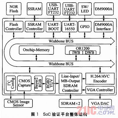
The OR1200 microprocessor is the control core of the entire verification platform. According to the requirements of the system and the principle of saving, the instruction buffer (IC), data buffer (DC) and memory management unit (IMMU and DMMU) in the OR1200 are cut. Another important module in the SoC platform is Onchip-Memory. On-chip memory has strong data access capability and low power consumption, but its capacity is limited. It can only implement specific functions with small code size (such as hardware initialization, CPU booting, etc.). When these operations are completed, the processor will jump to the address memory execution code of the main memory SSRAM.
Among other peripheral modules, the UART-BOOT module only has one Wishbone master port, which is used to control CPU startup and program download. It does not need to assign an address. The address space allocation of other modules is listed in Table 1.
In the IP core shown in Figure 1, all of the following modules are available for free from the Opencores website: The UART-BOOT module is designed to make it easier to update and download software code and control the SoC platform during the verification process. Independent design; the image acquisition module can refer to the reference design of Youjing Technology Co., Ltd., but the data collected is in RGB format and needs to be converted to H. The YUV format required by the 264 encoder; in addition, since the MT9P031 image sensor inside the image acquisition module is progressively scanned, and H. The 264 encoder is encoded in macroblock order, so the controller of the SDRAM needs to be redesigned to meet the requirements of progressive write and macroblock read.
Many people have done research on building SoC systems based on embedded soft cores. This article focuses on H. The 264 encoder verifies the relevant self-designed modules.
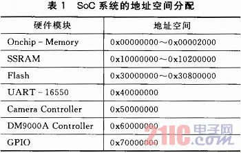
3 Multi-port SDRAM controller The overall structure of the multi-port SDRAM controller for progressive input/arbitrary macroblock sequential output is shown in Figure 2.
3.1 Read-Write Port and Read-Write Arbiter Figure 2 has a read port and a write port for H. The 264 encoder reads the data and the image acquisition module writes the data. In fact, there is also a read port for VGA display, the timing of which is the same as the write timing of the image acquisition module, which is a progressive scan, which is omitted here.
A read request from the read port and a write request from the write port are processed in a Read & Write Arbiter. The priority of the write request is higher than the priority of the read request. The write port consists of a write buffer (WE_FIFO) and a write address generator (WE_Addr Generator). The depth of the WE_FIFO is 512 words (32 bits per word, one pixel is stored). When the image acquisition module writes 256 words in the WE_FIFO, a write request is initiated. The write address generator increments by 256 after each write request is completed, and the order of address increase is the same as the scan order of the CMOS image sensor.
The read port consists of a read buffer (RD_FIFO), a read address generator (RD_Addr Generator), a read state machine (RD_FSM), and a row counter (Line_Cnt). The depth of the RD_FIFO is 256 words. After the command to load the macroblock address (addr_load) is issued, the RD_FSM enters the working state (the read_stat signal is 1). At the same time, the read address generator has calculated the base address in the SDRAM in which the macroblock is located based on the horizontal position (mb_num_h) and the vertical position (mb_num_v) of the macroblock. When RD_FSM is in the working state, the read request is always valid. If the write request is invalid at this time, a burst read transfer of length 16 is initiated, and 16 pixel data is read from the SDRAM to the RD_FIFO. When a read transfer is completed, the read address generator automatically increments the length of one line (configurable, here 800), which is the base address of the next line of the current macroblock. At the same time, the Read&Write Arbiter module will detect whether the write request is valid. If it is valid, it will initiate a burst write transfer of length 256, and then complete the next burst read transfer of length 16 after the write transfer is completed. Thus, when 16 burst read transfers are completed, the data of the read macroblock is completely written into the RD_FIFO. At this time, the RD_FSM changes from the working state to the idle state, waiting for the next macroblock read request.
When the amount of data (rd_usedw) in the RD_FIFO is not zero, H. The 264 encoder can read data from the RD_FIFO. When 256 data, that is, the data of one macro block, is read, the value of rd_u sedw becomes zero, and a macro block data is read.
3.2 SDRAM Command Generator and Command Arbiter The main function of the SDRAM Command Generator is to generate control commands at the SDRAM interface based on the control timing of the SDRAM. These commands are likely to conflict. The role of the Command Arbiter is to arbitrate commands generated by the command generator.
The initialization process of the SDRAM can be divided into four stages of initialization delay, precharge, refresh, and set mode registers, which are controlled by an initial timer. The SDRAM command generator generates an initialization delay command, a precharge command, a refresh command, and a set mode register (load_mode) command according to the value of the initialization counter. The refresh command may also be generated according to the value of the refresh timer during the operation of the SDRAM. This is because the characteristics of SDRAM require that all rows of SDRAM be refreshed every 64 ms. Since the SDRAM works in the automatic precharge mode in this design, it is said that the precharge command will only appear during the initialization process.
The command generator also generates read/write commands based on read and write requests from Read&Write Arbiter. The read/write command has the lowest priority. When the SDRAM controller is in the initialization process or is executing a refresh command, the command arbiter will wait for the read and write requests to wait for the higher priority command to complete. In addition, since the SDRAM is operating in the full-page mode, it is necessary to generate a burst termination command according to the burst length of the write or read. The burst termination command is generated based on the values ​​of the write timer and the read timer, which have a lower priority than the refresh command but higher than the read/write command.
4 SoC platform software support According to the reference, the control port of DM9000A is designed, and the μC/OS-II real-time operating system and μC/TCP-IP protocol stack are transplanted on the designed SoC platform. This is for the convenience of H. The bit stream data generated by the 264 encoder is transmitted to the PC for further verification.
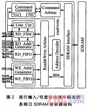
5 Experimental results A H. 264 encoder model, its main function is to simulate H. The read timing at the interface of the 264 encoder and the SDRAM controller reads data from the SDRAM. At the same time, it also has a Wish-bone slave interface, which can transfer the read data to the OR1200 microprocessor. The OR1200 microprocessor then transfers the image data to the PC through the network port to verify whether the read data is correct. The designed module was simulated by the Wishbone bus function model (BFM) in the ModelSim SE 6.5f environment. The verification scheme is shown in Figure 3.
In addition, Altera's Cyclone II series FPGA EP2C70F896C6 was selected for the entire SoC system and implemented on the DE2-70 development board of Taiwan Youjing Technology. The resources occupied by the entire platform are: 662 logical units, 689 registers, and 418104 bits.
Set the clock of the image acquisition module to 25 MHz, the clock of the SDRAM controller to 100 MHz, and the other modules to run at 50 MHz. In the foregoing method, the YUV image data collected in the order of the macroblocks from the SDRAM controller is transmitted to the PC through the network port, and the YUV image data is converted into a normal image sequence on the PC side, and the Y component is converted into a grayscale bitmap. The format is displayed and compared with the image displayed in the VGA display (the RGB channel is input with the transformed Y component).
Conclusion This article is based on the OR1200 microprocessor designed a H. The SoC verification platform of the 264 video encoder is based on the integration of various commonly used IP cores, with emphasis on H. The 264 encoder feature related multi-port SDRAM controller was designed. After RTL level and FPGA verification, the designed platform can meet H. The various requirements of 264 encoder software and hardware co-verification can greatly shorten H. 264 encoder development time.
Military power system refers to the power supply which can provide power for many equipments or other use ,as this items developed through our company R&D department,it has a high energy density and high working power.Seconldy as a new energy it uses ,it is totally pollution-free.Thirdly ,for this miltifunction power pack , Capacity, resistance, Voltage, platform time consistency is good.With short-circuit production function, it get more safe and reliable.Besides YFJ company has a very strict test before sending to customers in order to ensure of our product quality .
Charging chip protection
plate(using military-grade smart IC chip, with overcurrent, overpressure,
overcharge, overcharge, undervoltage, short circuit, reverse connection,
equilibrium voltage and equilibrium charging and other multiple protection
functions) to ensure the safety and reliability of the Battery Pack.
1. Solar panel: 18V/40W poly with 5m cable
2. Battery: 12V*40Ah Lithium Battery3. Output power: 500W inverter
4. Charging time: 4 hours
5. Extra battery voltage: DC12V
6. DC output: 5V/2A and 12V/5A
7. DC input: 12V/5A (PV charger)
8. Input voltage (Max): 24V
9. LED Lamp: 3W led lamp with 5m cable*2pcs
10. Lighting time: 74 Hours (2 lamps)
11. USB output: 5V/4A*4pcs
12. 4 in 1 charging kit: 1 set
13. AC output: 220V/50Hz or 110V/60Hz
14. Car boot port voltage: 12V/600A(instant current)
15. Storage time: 6 months
16. Operation Humidity: 10%RH-90%RH
17. Protection grade: IP42
18. Charge operating temperature: 0-45°C
19. Discharge operating temperature: -10~50°C
20. Certification: CE\FCC\UN38.3\ROHS
21. Dimentions: 480*305*165mm/power box
22. Weight: 8.5kg for power box, 13KG for whole set
23. Color option: Red and white, Yellow and white

Military Power Systems,Military Power Supply,Battery Power Supply,Adjustable Power Supply
YFJ TECHNOLOGY (HK) CO.,LIMITED , http://www.yfjpower.com