This article uses the clock chip DS1302 as an example to analyze the timing diagram and write the code. The DS1302 uses the SPI three-wire interface to communicate synchronously with the microcontroller. Focus on single-byte read timing, single-byte write timing, register read timing, register write timing, and complete four functions. Complete code and simulation map download address:
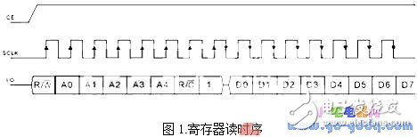
The above picture shows the register read timing. Why do you post this picture first because the read register contains a single-byte write and a single-byte read. As can be seen from the figure, reading the register of the DS1302 is to write an address first, and then read a byte. Then you can complete single-byte read and write timing analysis and code writing based on this graph.
Single byte write timingFigure 1 can tell us that on the rising edge of the clock is the write data, starting from the low bit. Another point to note is the write byte and read byte connections. As you can see from the figure, when the last bit is written, the next falling edge begins to read the data. Note this, otherwise reading the data will be wrong. Take a look at the following code:
Void dsWriteByte(u8 dat) //write byte
{
U8 i;
For(i = 0;i < 8;i++)
{
If(dat & 0x01) ds1302IOStatu(1);
Else ds1302IOStatu(0); //lower bit first write, determine the level of IO according to the data to be written
ds1302CLKStatu(0);
ds1302CLKStatu(1); //Generate a rising edge to write data
Dat >>= 1; //Shift, prepare the next one
}
} // After writing a byte, the clock pin is high
Solar On and Off Grid Inverter
Grid Tie Inverter,Solar Pump Inverter,On Grid Solar Inverter,On And Off Grid Inverter
Jinan Xinyuhua Energy Technology Co.,Ltd , https://www.xyhenergy.com