Working Principle and Application of LM567 Universal Tone Decoder Integrated Circuit
567 is a general-purpose tone decoder. It provides a saturation transistor to ground switch when the input signal is in the passband. The circuit consists of I and Q detectors. The voltage-controlled oscillator drives the oscillator to determine the center frequency of the decoder. Independently set the center frequency bandwidth and output delay with external components.
Mainly used for oscillation, modulation, demodulation, and remote control coding and decoding circuits. Such as power line carrier communication, interphone sub-audio decoding, remote control, etc. 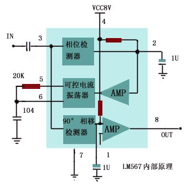
Logic compatible output with external resistor 20 to 1 frequency range has the ability to absorb 100mA current.
Adjustable bandwidth from 0% to 14%
Wide signal output and high noise suppression, anti-interference to false signals, high stable center frequency, center frequency adjustment from 0.01Hz to 500kHz
The power supply voltage is 5V-15V, 8V is recommended.
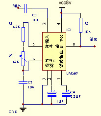
Application example: the input terminal is connected with a 104 capacitor, the output terminal is connected with a pull-up resistor of 10K, and C1 and C2 are 1uF. R1, C1 determine the oscillation frequency, generally C1 is 104 capacitors, R1 is 10K-200K. The power supply voltage is 8V.
The single-channel infrared remote control circuit can use the single-channel infrared remote control circuit composed of conventional integrated circuits in applications that do not require multi-channel control. This remote control circuit does not require the use of a more expensive dedicated codec, so the cost is lower.
The single-channel infrared remote control transmitter circuit is shown in Figure 1. A high-speed CMOS-type quadruple-input NAND gate 74HC00 is used in the transmitting circuit. Among them, NAND gates 3 and 4 form a carrier oscillator, and the oscillation frequency f0 is adjusted to about 38kHz; NAND gates 1 and 2 form a low-frequency oscillator, and the oscillation frequency f1 does not need to be adjusted accurately. f1 modulates f0, so the waveform output from the NAND gate 4 is an intermittent carrier wave, which is also the waveform transmitted by the infrared light-emitting diode. The waveforms of several key points are shown in Figure 2. The B 'waveform in the figure is the waveform output at point B when the A point is directly connected to the high level without the modulation waveform. It can be seen from Figure 2 that when the waveform at point A is at a high level, the infrared LED emits a carrier; when the waveform at point A is at a low level, the infrared LED does not emit a carrier. This stop frequency is the low frequency oscillator frequency f1. Why not use the low-cost low-speed CMOS quadruple-input NAND gate CD4011 in the infrared emission circuit, but the higher price 74HC00? Mainly due to the limitation of the power supply voltage. The shell of the infrared transmitter is various, but the power supply is generally designed to be 3V, and two batteries of No. 5 or No. 7 are used as the power source. Although the nominal operating voltage of the CD4011 is 3 to 18V, it is for processing digital signals. Because the CMOS NAND gate here is used to oscillate a square wave signal, that is, an analog application, its operating voltage must be at least 4.5V, otherwise it will not be easy to vibrate and affect its use. The 74HC series of CMOS digital integrated circuits have a minimum operating voltage of 2V, so using a 3V power supply is "handy." The pin function of 74HC00 is shown in Figure 3. 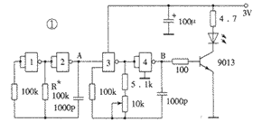
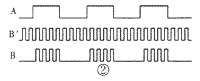

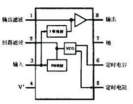
Figure 4 shows the infrared receiver demodulation control circuit. In the figure, IC1 is LM567. LM567 is a phase-locked loop circuit, using 8-pin dual in-line plastic packaging. The external resistance and capacitance of the ⑤ and ⑥ feet determine the center frequency f2 of the internal voltage controlled oscillator, f2≈1 / 1.1RC. The ①and ② pins are usually grounded through a capacitor to form an output filter network and a loop single-stage low-pass filter network. ② The capacitor connected to the pin determines the capture bandwidth of the phase-locked loop: the larger the capacitance value, the narrower the loop bandwidth. ①The capacitance of the capacitor connected to the foot should be at least twice that of the foot capacitor. ③The foot is the input terminal, and the input signal is required to be ≥25mV. ⑧The foot is a logic output terminal, and its inside is an open collector transistor, which allows a maximum sink current of 100mA. The working voltage of LM567 is 4.75 ~ 9V, the working frequency is from DC to 500kHz, and the static working current is about 8mA. The internal circuit and detailed working process of the LM567 are very complicated. Here, only the basic functions are summarized as follows: When the LM567 pin input signal with amplitude ≥25mV and frequency within its bandwidth, ⑧ pin changes from high level to low level , ② pin outputs the modulated signal with frequency / voltage conversion; if the audio signal is input to the ② pin of the device, the FM square wave signal modulated by the ② pin input modulation signal is output at the ⑤ pin. In the circuit of Fig. 4, we only use the characteristic that the LM567 receives the carrier signal of the same frequency ⑧ pin voltage from high to low to form the control of the control object. 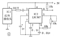
After clarifying the basic working principle and function of LM567, it is very simple to analyze the circuit of Figure 4 again. IC1 is an infrared receiver. It receives the infrared signal from the transmitter. Its center frequency is the same as the carrier frequency f0 of the transmitter. After demodulation by IC1, it outputs a square wave signal of frequency f1 at the output terminal OUT, which is the same as Figure 1. The signal with the same waveform at point A. We tune the center frequency of the LM567 to the same oscillation frequency as the NAND gates 1 and 2 in the transmitter, even if f2 = f1. Then, when the transmitter emits a signal, the LM567 starts to work, and the foot changes from high level to low level. This changed level can be used to control various objects. Using the circuit in Figure 4, we can make a remote control switch to remotely control various household appliances in the home.
In fact, using the circuits shown in Figure 1 and Figure 4, we can also easily transform it into a multi-channel remote control circuit. The method is: change the resistance R * into several different values ​​in the transmitter (Figure 1), thereby forming several kinds of modulation signals with different frequencies; in the receiving circuit, set up a few LM567, the input of which is from infrared receiver At the head, the oscillation frequency of each LM567 is different but corresponds one-to-one with the transmitter. In this way, when the transmitter presses different buttons and accesses different modulation signals, the level of the ⑧ foot of the LM567 corresponding to the receiving end will change, thereby forming multiple control. Strictly speaking, this is a kind of frequency division multiplexing. Compared with digital coding and decoding multiplexing, the disadvantage is that the debugging is more complicated. But on some occasions, such as in multi-channel alarms, there is also a place. In an alarm application, when it is necessary to solve the problem of more than two simultaneous alarms, there is a complicated synchronization problem when using time division multiplexing, and frequency division multiplexing is easy to solve if the bandwidth allows.
Ultrasonic remote control circuit 1. Ultrasonic remote control light switch This remote control switch has a simple circuit and no debugging, which is very suitable for beginners.
1. The working principle is the transmitting circuit. The circuit is composed of discrete devices. VT1 and VT2 and R1 ~ R4, C1 and C2 constitute a self-excited multivibrator. The ultrasonic transmitting device B is connected to the collector circuit of VT1 and VT2 and works in a push-pull form. Determined by R1, C1 and R4, C2. The resonance frequency of the ultrasonic transmitting device B triggers the multi-resonant oscillation circuit. Therefore, this circuit can work at the best frequency. 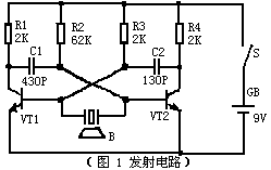
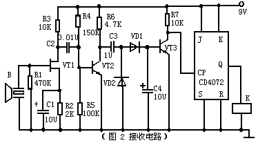
(Figure 2) For the receiving circuit, the junction field effect VT1 constitutes a high input impedance amplifier, which can be well matched with the ultrasonic receiving device B, and can obtain higher receiving sensitivity and frequency selection characteristics. VT1 adopts self-sufficient bias method. Changing R3 can change the apparent operating point of VT1. Ultrasonic receiving device B converts the received ultrasonic waves into corresponding electrical signals, which are amplified by the two poles of VT1 and VT2. The rectification becomes a DC signal, which acts on VT3 and the base after being integrated by C3, so that VT3 changes from cut-off to conduction, its collector outputs a negative pulse, and trigger JK triggers D to turn it over. The level of the Q terminal of the JK trigger directly drives the relay K, causing K to pull in or release. The switch of the circuit is controlled by the contact of the relay K.
Second, the components are selected in the transmission circuit, VT1 and VT2 use CS9013 or CS9014 and other small power transistors, ≥100. The ultrasonic transmitting device uses SE05-40T, and the power supply GB uses a 9V laminated battery to reduce the size and weight of the transmitter.
In the receiving circuit, VT1 and 3DJ6 or 3DJ7 and other small power junction field effect transistors. CS9013 is used for VT2 ~ VT3, ≥100. Use IN4148 for VD1 and VD2. JK trigger 263B. The ultrasonic receiving device uses SE05-40R, which is paired with SE05-40T. Relay K uses HG4310 type.
Ultrasonic remote control electric fan transmission 1. Working principle
(Figure 3) is the transmitter circuit. It uses the remote control transmitter of the domestic bat brand FS-A5A electric fan. This kind of transmitter has the characteristics of small size, low power consumption, reliable operation and simple circuit. In use, every time you press the transmit button, the transmitter emits 40KHZ ultrasonic waves for about 500ms. The working principle of the transmitting circuit is as follows. 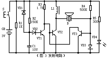
VT2 and VT3 form a direct-coupled positive feedback oscillation circuit, B is a 40KHz ultrasonic transmitting device, and also feeds back to the pre-frequency component of the oscillation circuit. Therefore, this circuit can accurately oscillate at the center frequency of 40KHZ of the ultrasonic transmitting device. VT1 and R2 and C1 form a 500ms delay circuit. R1 and VD1 are the discharge path of C1. When the transmit key S is pressed, the oscillating circuit formed by VT2 works and emits ultrasonic waves. At the same time, the power is charged to C1 through R2. When the potential on C1 reaches 1.4V (about 500ms ), VT1 is turned on, the potential of the base of VT2 and the collector of VT3 drops to about 0.3V, and the oscillator stops working.When the launch button S is released, C1 quickly discharges through VD1 and R1 to prepare for the next launch. And R4 constitute the emission instruction circuit. When the emission key is pressed, VD3 emits light.
(Figure 4) is the receiving circuit. CMOS NOT gates D1 ~ D3 are biased as linear amplifiers by R1, and the total gain can reach more than 60bB. Due to the high input impedance of the CMOS circuit, it can be well matched with the ultrasonic receiving device. The amplified signal is coupled to the input pin 3 of the phase-locked loop decoder LM567 by C1. When the frequency of the input signal falls on its center frequency, the pin 8 of the logic output of the LM567 changes from high level to low level. 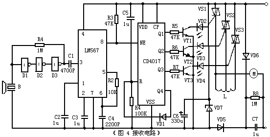
Frequency-selective voice-activated switch This voice-activated switch can control the turning on or off of any electrical appliance by a specific tone (500 to 2000 Hz) sound. Because it has a certain frequency selection effect, the probability of misoperation is small.
The circuit is designed to be controlled with audio electrical signals (up to 100mV), and the control signal source can be a telephone, radio, record player, recorder, and the appropriate points from them are drawn with shielded wires. If you want to use sonic remote control, add an electret microphone and a level of pre-amplification.
The circuit of this device is shown in Figure 16. Its central device is a pickup integrated circuit LM567, and a 50mA relay.
After the audio signal of a certain tone is added to the input terminal (3 feet) of the LM567, after the internal circuit amplification, frequency selection and other processing, it outputs a low level at its output terminal 8 (high level when there is no input signal). At this time, a PNP tube (2N3906) connected to it is turned on, so that the relay connected in the collector circuit is attracted, so as to control the controlled appliance with its contact point. If it is used for starting, the normally open and dynamic closing contacts of the relay are used; if it is used for shutting down, the normally open and dynamic opening contacts should be used.
The response frequency depends on the value of the potentiometer and capacitor connected to the 5th and 6th pins, so adjust the 10kΩ potentiometer to adjust its response frequency. The audio range that this machine can receive is 500 ~ 2000Hz.
Diode 1N4001 is used to protect the transistor. 2N3906 can be replaced by any other type of medium and low power PNP silicon tube. 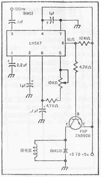
The Work Light is Ideal for mechanic's, DIY, boating, camping, night fishing ,Camping, Hiking, Workshop, Roadside safety, Auto repair, Emergency kits, Survival device, Home security etc.
Both Work Light's Base and Body have strong magnet to magnetize on metal surfaces for more convenience; Use Hook to hang on any place to provide brightness.
The Opereating Time of work light up to 6 Hours As Per One Fully Charged, It can Also be Used as a Backup Battery to Charge Your Phone or Other Digital Device.
Work Light
Work Lights,Extendable Work Light,Rotating Work Light,Switch Light
Ningbo Henglang Import & Export Co.,Ltd , https://www.odistarflashlight.com