Abstract: This arTIcle helps the designer of a data converter system to select the proper input buffer to achieve opTImum performance. Numerous parameters and their effect on data converter performance are discussed including; noise, distorTIon, bandwidth, settling TIme, gain flatness, slew rate , SFDR, current drive, offset voltage, loop gain, and output impedance.
Selecting the optimum drive amplifier (or buffer) for a specific analog-to-digital converter (ADC) requires attention to impedance matching, charge injection, noise reduction, and output accuracy. ADC manufacturers often recommend a specific amplifier for a given converter, but the combination must be compatible with the target system. Overall performance must be considered as well as the ADC's input structure and its effect on the buffer.
Progress in the development of ADCs—including ever-increasing speed and resolution, switched-capacitor input structures, and single-supply operation—is forcing system designers to evaluate the associated drive amplifier very carefully. The drive amplifier, or buffer, must provide a low source impedance and sufficient output current to drive the ADC inputs, and its high-frequency output impedance must be sufficiently low to avoid excessive conversion error. For many sampling ADCs, the buffer also must amplify extremely low-level signals. How Noise Affects PerformanceIdeally , an op-amp signal source should contribute no error beyond that of the ADC. As a minimum condition for avoiding excess noise in the system, the signal-to-noise ratio (SNR) of the source should be better than the theoretical limit of the ADC. Fortunately, the noise performance of all new-generation op amps is much better than 12 bits, and those with good 16-bit noise performance are not difficult to find. It's imp ortant to note, however, that the noise powers of the amplifier and the ADC are cumulative.
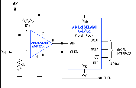
Figure 1. This interface between a drive amplifier and a 16-bit ADC offers low noise and low distortion.
Figure 1 is an excellent example of a low-noise, low-distortion interface between a 16-bit successive-approximation ADC (MAX195) and its input drive amplifier (MAX4256). For this example, calculate the total RMS noise contributed by the buffer using information from the MAX4256 data sheet:
Input voltage-noise density
eN = 7.9nV / | Hz, at Æ’ = 30kHz
Input current-noise density
iN = 0.5 Æ’ A / | Hz, at Æ’ = 1kHz.
Because the effective noise bandwidth of a single-pole filter is 1.57 times the -3dB corner frequency, the MAX4256's noise bandwidth is GBW / 1.57AV. In addition to voltage-noise and current-noise sources in the IC, each resistor in the circuit contributes a noise voltage. Thus, the total equivalent input-referred noise is:
That is, total noise =
To simplify calculation, remember that the noise generated by a 1kΩ resistor in a 1Hz bandwidth is 4nVRMS. That information reduces the formula t

where Req (BW) is the equivalent resistance in a specified bandwidth. Assuming a bandwidth of 20kHz for this typical audio-frequency application, and bearing in mind the MAX195 sampling rate (85ksps), the result is eN = 8.7nV / | Hz. Note that the MAX4256's input current noise of 0.5 Æ’ A / | Hz is insignificant in comparison. Total output noise referred to the op-amp circuit's bandwidth is:

To determine the total noise power for the ADC / op-amp combination, first convert the ADC signal noise and distortion (SINAD) values ​​from decibels to voltage. Then calculate the square root of the sum of the squares and convert the value back to decibels In this case, we use the MAX195's minimum guaranteed SINAD value of 87dB. Converting to voltage (44.7µV) and combining with ET = 17µV results in a total noise power of 86.4dB-a degradation of only 0.6LSB in the ADC's SNR. A series of these calculations can demonstrate the effect of a given drive amplifier on the overall performance. DistortionDistortion also degrades dynamic performance, but this effect can be minimized by choosing an amplifier whose distortion is much less than the converter's total harmonic distortion (THD). Again, Figure 2's circuit is very effective: the MAX195's THD is only -97dB (0.0014%), and the MAX4256's SINAD is an outstanding -115dB. This high performance allows use of the noninverting configuration and a single-supply op amp (MAX4256).
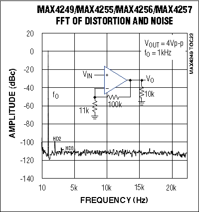
Figure 2. The MAX4256 offers an outstanding spurious-free dynamic range (SFDR) of 115dB.
Another way to evaluate op amps as drive amplifiers is to compare their numerical specifications to the weight (step size) of the ADC's least significant bit (LSB) in volts. For example, the LSB for a 16-bit ADC with a 5.000V unipolar input range is 76µV. To approximate the amplifier's error contribution, compare that number to the amplifier's input offset voltage, drift, and noise, all multiplied by its closed-loop gain. Thus, a closed-loop gain of + 11V / V and an offset of 70µV (typical for the MAX4256) produce an error of 770µV, which for a 16-bit application is 10LSBs! If DC accuracy is important, the buffer's offset must either be much less than the ADC's maximum offset (± 3LSBs for the MAX195 ), or it should be trimmed through hardware or software.
The MAX410 family op amps also work well with the ± 5V supplies used by the MAX195. The MAX410 has a ± 3.5V common-mode input range and a similar output-voltage swing, which allows the converter to operate with reference voltages up to 3.5 V. The MAX410's offset voltage (250µV) is approximately 2LSBs. Its drift (1µV / ° C), unity-gain bandwidth (28MHz), and low voltage noise (2.4nV / Hz) are all compatible with 16-bit performance ( Figure 3).
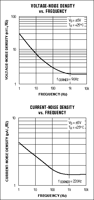
Figure 3. Voltage- and current-noise density graphs (for the MAX410) aid in calculating the accuracy obtainable with a given ADC. Bandwidth and Settling TimeTo determine speed requirements for the drive amplifier, match its settling time to the ADC's acquisition time. That is, the conversion results will be accurate if the ADC samples the input signal for an interval longer than the amplifier's worst-case settling time. By definition, settling time is the interval between the application of an input voltage step and the point at which the output signal reaches and stays within a given error band centered on the resulting steady-state output level (Figure 4).
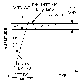
Figure 4. Output settling time is defined with respect to an error band centered on the final settled value.
For large input steps, the amplifier's slew-rate limit restricts the speed with which its output can change. The result, for a given input amplitude and for an amplifier with a given slew rate, is a maximum at the frequency that can be faithfully reproduced :
Æ’MAX = SR / 2Ï€ Vp
where Vp is the peak output voltage.
A first-order approximation of settling time (tS) can be made if the following conditions apply: The input signal does not cause the amplifier output to enter slew-rate limiting The amplifier's -3dB corner frequency is known The output amplitude rolls off at 20dB / decade for at least one decade of frequency above Æ’ -3dB. Then,
tS = -1 / 2πƒ-3dB [ln (VO / VS-1)] [1]
To calculate tS to within 1 / 2LSB at N-bit resolution, replace VO / VS with the expression (2N-1/2) / 2N, where N is the number of bits. Equation [1] now becomes:
tS = 0.11 (1 + N) / Æ’ -3dB [2]
Finding an amplifier that meets the requirements of your application may be difficult. Numerous op amps can operate satisfactorily with 12-bit ADCs, but only a few are suitable for driving 14- and 16-bit ADCs above 500kHz. The choice involves trade-offs among the parameters of noise, distortion, and settling time. Settling time poses a problem because few op-amp manufacturers test this specification at levels equivalent to 16-bit performance (0.001%).
Consider bandwidth and settling time for the drive amplifier in Figure 1. For its typical slew rate of 2.1V / µs, the maximum frequency this buffer can handle with an input amplitude of 2Vp-p is ƒ MAX = SR / 2π 2Vp = 167kHz. Similarly, for settling time, solve equation [2] for the ƒ -3dB frequency after substituting the 16-bit settling time (1.6µs at 0.001%) for tS. Though just an approximation, the surprising result is 1.17MHz. Bandwidth requirements for high-resolution settling time can be much higher than expected, and designers often underestimate the bandwidth necessary to sustain gain accuracy. Insufficient gain over the input-signal bandwidth can easily introduce errors greater than 1LSB. Fortunately, the MAX4256 offers a -3dB corner frequency of 22MHz. High-Speed ​​ApplicationsFor demanding video and other high-speed applications, Maxim offers a broad range of video op amps that are also suitable for use as ADC drivers. Among them, the members of a new family of low-noise, low -d istortion, 880MHz video op amps make outstanding drive amplifiers (Table 1 and Figure 5):
Table 1. Op amp family for ADC driver applications
 -3dB bandwidth of 880MHz (MAX4104) 0.1dB gain flatness to 100MHz (MAX4104 / MAX4105) 1400V / µs slew rate (MAX4105 / MAX4305) Spurious-free dynamic range (SFDR) (5MHz, RL = 100Ω) of -88dBc (MAX4104 / MAX4304) High output-current drive: ± 70mA Low input offset voltage: ± 1mV
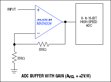
Figure 5. This op amp is configured as an ADC buffer with a noninverting gain of + 2V / V.
Also noteworthy as drive amplifiers are the MAX4106 / MAX4107 op amps, which combine high speed with an ultra-low noise level of 0.75nV / | Hz. The MAX4106 is compensated for closed-loop gains of + 5V / V or greater, the MAX4107 for + 10V / V or greater. Low-distortion architecture provides an SFDR of 63dB at 5MHz. Furthermore, these high-speed op amps have a wide output-voltage swing (± 3.2V with a ± 5V supply) and a substantial current- drive capability of 80mA (Figure 6).
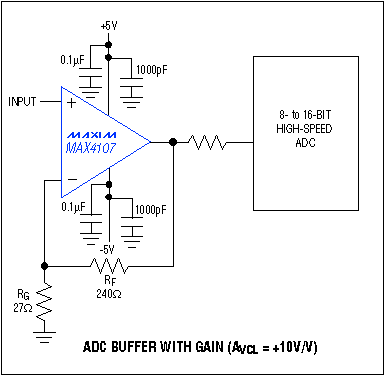
Figure 6. Operating with a noninverting gain of + 10V / V, this ADC buffer suits high-frequency applications.
Finally, the MAX4108 / MAX4109 / MAX4308 / MAX4309 op-amp family combines ultra-high speed with ultra-low distortion. At 5MHz, VOUT = 2Vp-p and RL = 100Ω, the MAX4108 SFDR is an unprecedented -93dBc. High speed, high slew rate, low (or ultra-low) noise, and low, stable distortion levels make these op amps well suited for use as buffer amplifiers in high-speed ADC applications (Figure 7).
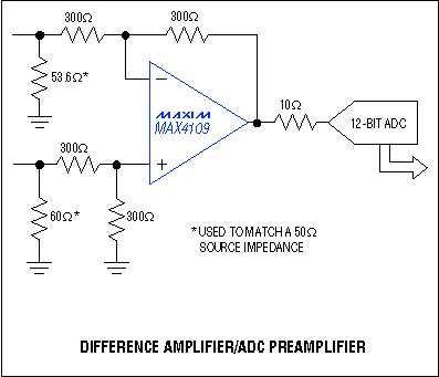
Figure 7. The buffer in this high-speed ADC application operates as a difference amplifier / preamplifier. Buffer Performance also Depends on the ADC Input Structure In addition to the considerations discussed above, a key concern in selecting a buffer (drive amplifier) ​​is the ADC's input structure. For example, flash converters are among the most difficult to drive because they have a large nonlinear input capacitance. ADCs that have the newer switched-capacitor architectures also require close attention.
The task of driving a switched-capacitor ADC is simplified if you recognize that the ADC draws a small transient of input current at the end of each conversion, when the internal sampling capacitors switch back to the input for acquisition of the next sample. To avoid errors, the buffer circuitry must recover from this transient and settle before the next conversion starts. This can be accomplished using either of two methods.
One method requires driving the ADC with an op amp that settles from a load transient in less than the ADC's acquisition time. (Many new ADCs include such wideband sample / holds on-chip.) Fortunately, most op amps settle from a load transient much more quickly than from an input step, so this requirement is not too difficult to meet with an external buffer. A second method involves adding an RC filter at the input whose capacitor is much larger than the ADC's input capacitance. This larger capacitor eliminates the transient by providing charge for the sampling capacitor (Figure 8). To absorb transient glitches, Maxim often recommends using a capacitor of 1000pF or more between the ADC input and ground.
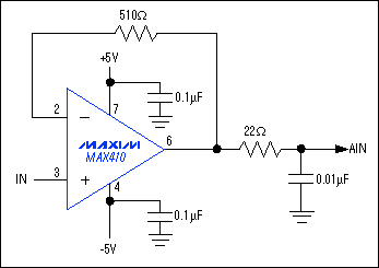
Figure 8. The 22Ω / 0.1µF output filter absorbs transients from the ADC and helps stabilize the amplifier.
An RC filter also reduces the possibility of amplifier-stability problems when driving a capacitive load. A small resistor in series with the capacitor helps to prevent ringing and oscillation. At higher capacitive loads, AC performance is controlled by the interaction of the load capacitance and the isolation resistor.
Another key concern is to ensure that the amplifier maintains low output impedance over all input frequencies of interest. Op amps with high output impedance cannot respond quickly to changes in the ADC's input capacitance. Nor can they handle the transient currents produced by the ADC. Nonlinearities result when the op amp does not settle in time for the next conversion.
Remember that high loop gain is necessary for low output impedance, according to the equation ROUT = RO / (1 + AVOβ), where RO is the open-loop output impedance and AVOβ is the loop gain. AVOβ decreases as you approach the op amp's Unity-gain crossover frequency, leading to increased output impedance (Figure 9). Higher output impedance makes it difficult for the amplifier to handle current spikes from the ADC.
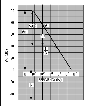
Figure 9. Output impedance generally rises with frequency.
Thus, the low-impedance requirement leads to a requirement for wide bandwidth. Because higher bandwidth op amps have higher loop gain and therefore lower output impedance at higher frequencies, it makes sense to use a 500MHz op amp in front of a 50Msps ADC. The high-bandwidth op amp is more effective than a lower bandwidth amplifier in absorbing current transients produced by the ADC. Limited Loop Gain Error Can Affect Overall Gain AccuracyThe Bode diagram of Figure 9 also depicts, for the noninverting circuit, the relationships between open-loop gain (A), the feedback-attenuation factor (β), noise gain (1 / β), and loop gain (Aβ, or AVOβ at DC) as functions of frequency. Figure 9 shows the variation of open-loop gain vs. frequency for a typical operational amplifier. At very low frequencies, the DC open-loop gain (AVO) is near 100dB. Also note that the logarithm of the feedback-attenuation factor is negative because it represents a reduction in the signal amplitude.
Loop gain is depicted in the figure as the sum of the open-loop gain and the feedback attenuation factor (+ 100dB + (-40dB) = 60dB at very low frequency), or as the difference between the open-loop gain and the noise gain, 1 / β [+ 100dB-(+ 40dB) = 60dB]. For a given value of β, observe that as frequency increases, the loop gain Aβ decreases. To obtain a greater amount of loop gain at higher frequencies, either increase the open-loop gain of the amplifier or increase the feedback factor β (ie, decrease the noise gain).
These observations lead to a key equation in feedback systems. Referring to the unity-gain noninverting amplifier,
ACL = VOUT / VIN = 1 / (1 + 1 / Aβ). [3]
This equation indicates that the closed-loop gain (ACL) depends on both the open-loop gain and the feedback factor. Both of these quantities are functions of frequency, so loop gain is a function of frequency as well. The amount of loop gain at the operating frequency is the key measure of how closely an amplifier configuration approaches the ideal.
To understand the effect of open-loop gain on overall gain accuracy, consider a practical example based on equation [3]. Assuming an op amp with 40dB open-loop gain at the frequency of interest, the closed-loop gain has an error of 1%. This error drops to 0.1% at 60dB gain, and to 0.01% at 80dB gain. Therefore, 80dB is the minimum allowable open-loop gain that will maintain unity closed-loop gain while properly driving a 12-bit ADC. To accommodate a higher closed-loop gain, modify equation [3] as follows:
ACL = VOUT / VIN = (1 / (1 + 1 / Aβ)) (RF + RI) / RI [4]
where RF and RI are the feedback and input resistors, respectively. Depending on the level of closed-loop gain required, even higher open-loop gain may be needed to maintain the required accuracy. Output Impedance vs. FrequencyLow impedance vs. frequency has made video amplifiers such as the MAX4100 very popular as ADC drivers in medical ultrasound applications (Figure 10). At the sampling frequency typical for the newest 10-bit ADCs in ultrasound systems (50MHz), the MAX4100 exhibits an output resistance of less than 2Ω. The MAX4100 is a voltage-feedback, high-speed, unity-gain-stable amplifier that delivers a 500MHz unity-gain bandwidth, a 250V / µs slew rate, and a settling time of 35ns (to 0.01%) or 18ns (to 0.1 %).
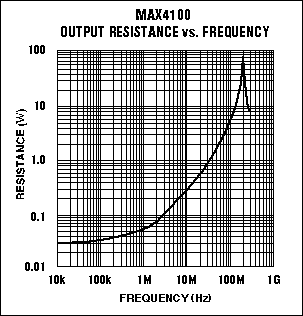
Figure 10. The MAX4100 exhibits less than 0.2Ω output resistance at 50MHz.
Despite the availability of new ADC architectures and other technology improvements, companies like Maxim answer many questions about missing codes and poor linearity. The cause of these problems is generally assumed to be poor performance in the ADC, but it often stems from a poor choice of drive amplifier instead. Tables 2 and 3 give an overview of the ADC-drive amplifiers, enabling a selection of single-supply (down to + 2.7V) vs. dual-supply types, and fastest vs. most-accurate types.
Table 2. ADC drive-amplifier selection, single op amps, single supply (+ 2.7V to + 5.5V)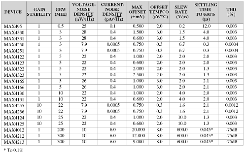
Table 3. ADC drive-amplifier selection, single op amps, dual supplies (± 5V) References Maxim Integrated Products, Full-Line Data Catalog on CD-ROM, 1998 Ed., Version 2.0. Crystal Semiconductor, Application Note AN06, January 1995. Linear Technology Corp., Application Note 71, July 1997. Burr-Brown Corp., Application Bulletin AB-098, April 1995.
Selecting the optimum drive amplifier (or buffer) for a specific analog-to-digital converter (ADC) requires attention to impedance matching, charge injection, noise reduction, and output accuracy. ADC manufacturers often recommend a specific amplifier for a given converter, but the combination must be compatible with the target system. Overall performance must be considered as well as the ADC's input structure and its effect on the buffer.
Progress in the development of ADCs—including ever-increasing speed and resolution, switched-capacitor input structures, and single-supply operation—is forcing system designers to evaluate the associated drive amplifier very carefully. The drive amplifier, or buffer, must provide a low source impedance and sufficient output current to drive the ADC inputs, and its high-frequency output impedance must be sufficiently low to avoid excessive conversion error. For many sampling ADCs, the buffer also must amplify extremely low-level signals. How Noise Affects PerformanceIdeally , an op-amp signal source should contribute no error beyond that of the ADC. As a minimum condition for avoiding excess noise in the system, the signal-to-noise ratio (SNR) of the source should be better than the theoretical limit of the ADC. Fortunately, the noise performance of all new-generation op amps is much better than 12 bits, and those with good 16-bit noise performance are not difficult to find. It's imp ortant to note, however, that the noise powers of the amplifier and the ADC are cumulative.
Figure 1. This interface between a drive amplifier and a 16-bit ADC offers low noise and low distortion.
Figure 1 is an excellent example of a low-noise, low-distortion interface between a 16-bit successive-approximation ADC (MAX195) and its input drive amplifier (MAX4256). For this example, calculate the total RMS noise contributed by the buffer using information from the MAX4256 data sheet:
Input voltage-noise density
eN = 7.9nV / | Hz, at Æ’ = 30kHz
Input current-noise density
iN = 0.5 Æ’ A / | Hz, at Æ’ = 1kHz.
Because the effective noise bandwidth of a single-pole filter is 1.57 times the -3dB corner frequency, the MAX4256's noise bandwidth is GBW / 1.57AV. In addition to voltage-noise and current-noise sources in the IC, each resistor in the circuit contributes a noise voltage. Thus, the total equivalent input-referred noise is:
That is, total noise =
To simplify calculation, remember that the noise generated by a 1kΩ resistor in a 1Hz bandwidth is 4nVRMS. That information reduces the formula t
where Req (BW) is the equivalent resistance in a specified bandwidth. Assuming a bandwidth of 20kHz for this typical audio-frequency application, and bearing in mind the MAX195 sampling rate (85ksps), the result is eN = 8.7nV / | Hz. Note that the MAX4256's input current noise of 0.5 Æ’ A / | Hz is insignificant in comparison. Total output noise referred to the op-amp circuit's bandwidth is:
To determine the total noise power for the ADC / op-amp combination, first convert the ADC signal noise and distortion (SINAD) values ​​from decibels to voltage. Then calculate the square root of the sum of the squares and convert the value back to decibels In this case, we use the MAX195's minimum guaranteed SINAD value of 87dB. Converting to voltage (44.7µV) and combining with ET = 17µV results in a total noise power of 86.4dB-a degradation of only 0.6LSB in the ADC's SNR. A series of these calculations can demonstrate the effect of a given drive amplifier on the overall performance. DistortionDistortion also degrades dynamic performance, but this effect can be minimized by choosing an amplifier whose distortion is much less than the converter's total harmonic distortion (THD). Again, Figure 2's circuit is very effective: the MAX195's THD is only -97dB (0.0014%), and the MAX4256's SINAD is an outstanding -115dB. This high performance allows use of the noninverting configuration and a single-supply op amp (MAX4256).
Figure 2. The MAX4256 offers an outstanding spurious-free dynamic range (SFDR) of 115dB.
Another way to evaluate op amps as drive amplifiers is to compare their numerical specifications to the weight (step size) of the ADC's least significant bit (LSB) in volts. For example, the LSB for a 16-bit ADC with a 5.000V unipolar input range is 76µV. To approximate the amplifier's error contribution, compare that number to the amplifier's input offset voltage, drift, and noise, all multiplied by its closed-loop gain. Thus, a closed-loop gain of + 11V / V and an offset of 70µV (typical for the MAX4256) produce an error of 770µV, which for a 16-bit application is 10LSBs! If DC accuracy is important, the buffer's offset must either be much less than the ADC's maximum offset (± 3LSBs for the MAX195 ), or it should be trimmed through hardware or software.
The MAX410 family op amps also work well with the ± 5V supplies used by the MAX195. The MAX410 has a ± 3.5V common-mode input range and a similar output-voltage swing, which allows the converter to operate with reference voltages up to 3.5 V. The MAX410's offset voltage (250µV) is approximately 2LSBs. Its drift (1µV / ° C), unity-gain bandwidth (28MHz), and low voltage noise (2.4nV / Hz) are all compatible with 16-bit performance ( Figure 3).
Figure 3. Voltage- and current-noise density graphs (for the MAX410) aid in calculating the accuracy obtainable with a given ADC. Bandwidth and Settling TimeTo determine speed requirements for the drive amplifier, match its settling time to the ADC's acquisition time. That is, the conversion results will be accurate if the ADC samples the input signal for an interval longer than the amplifier's worst-case settling time. By definition, settling time is the interval between the application of an input voltage step and the point at which the output signal reaches and stays within a given error band centered on the resulting steady-state output level (Figure 4).
Figure 4. Output settling time is defined with respect to an error band centered on the final settled value.
For large input steps, the amplifier's slew-rate limit restricts the speed with which its output can change. The result, for a given input amplitude and for an amplifier with a given slew rate, is a maximum at the frequency that can be faithfully reproduced :
Æ’MAX = SR / 2Ï€ Vp
where Vp is the peak output voltage.
A first-order approximation of settling time (tS) can be made if the following conditions apply: The input signal does not cause the amplifier output to enter slew-rate limiting The amplifier's -3dB corner frequency is known The output amplitude rolls off at 20dB / decade for at least one decade of frequency above Æ’ -3dB. Then,
tS = -1 / 2πƒ-3dB [ln (VO / VS-1)] [1]
To calculate tS to within 1 / 2LSB at N-bit resolution, replace VO / VS with the expression (2N-1/2) / 2N, where N is the number of bits. Equation [1] now becomes:
tS = 0.11 (1 + N) / Æ’ -3dB [2]
Finding an amplifier that meets the requirements of your application may be difficult. Numerous op amps can operate satisfactorily with 12-bit ADCs, but only a few are suitable for driving 14- and 16-bit ADCs above 500kHz. The choice involves trade-offs among the parameters of noise, distortion, and settling time. Settling time poses a problem because few op-amp manufacturers test this specification at levels equivalent to 16-bit performance (0.001%).
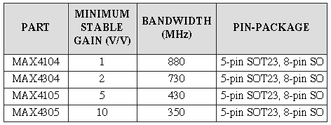
Consider bandwidth and settling time for the drive amplifier in Figure 1. For its typical slew rate of 2.1V / µs, the maximum frequency this buffer can handle with an input amplitude of 2Vp-p is ƒ MAX = SR / 2π 2Vp = 167kHz. Similarly, for settling time, solve equation [2] for the ƒ -3dB frequency after substituting the 16-bit settling time (1.6µs at 0.001%) for tS. Though just an approximation, the surprising result is 1.17MHz. Bandwidth requirements for high-resolution settling time can be much higher than expected, and designers often underestimate the bandwidth necessary to sustain gain accuracy. Insufficient gain over the input-signal bandwidth can easily introduce errors greater than 1LSB. Fortunately, the MAX4256 offers a -3dB corner frequency of 22MHz. High-Speed ​​ApplicationsFor demanding video and other high-speed applications, Maxim offers a broad range of video op amps that are also suitable for use as ADC drivers. Among them, the members of a new family of low-noise, low -d istortion, 880MHz video op amps make outstanding drive amplifiers (Table 1 and Figure 5):
Table 1. Op amp family for ADC driver applications
-3dB bandwidth of 880MHz (MAX4104) 0.1dB gain flatness to 100MHz (MAX4104 / MAX4105) 1400V / µs slew rate (MAX4105 / MAX4305) Spurious-free dynamic range (SFDR) (5MHz, RL = 100Ω) of -88dBc (MAX4104 / MAX4304) High output-current drive: ± 70mA Low input offset voltage: ± 1mV Figure 5. This op amp is configured as an ADC buffer with a noninverting gain of + 2V / V.
Also noteworthy as drive amplifiers are the MAX4106 / MAX4107 op amps, which combine high speed with an ultra-low noise level of 0.75nV / | Hz. The MAX4106 is compensated for closed-loop gains of + 5V / V or greater, the MAX4107 for + 10V / V or greater. Low-distortion architecture provides an SFDR of 63dB at 5MHz. Furthermore, these high-speed op amps have a wide output-voltage swing (± 3.2V with a ± 5V supply) and a substantial current- drive capability of 80mA (Figure 6).
Figure 6. Operating with a noninverting gain of + 10V / V, this ADC buffer suits high-frequency applications.
Finally, the MAX4108 / MAX4109 / MAX4308 / MAX4309 op-amp family combines ultra-high speed with ultra-low distortion. At 5MHz, VOUT = 2Vp-p and RL = 100Ω, the MAX4108 SFDR is an unprecedented -93dBc. High speed, high slew rate, low (or ultra-low) noise, and low, stable distortion levels make these op amps well suited for use as buffer amplifiers in high-speed ADC applications (Figure 7).
Figure 7. The buffer in this high-speed ADC application operates as a difference amplifier / preamplifier. Buffer Performance also Depends on the ADC Input Structure In addition to the considerations discussed above, a key concern in selecting a buffer (drive amplifier) ​​is the ADC's input structure. For example, flash converters are among the most difficult to drive because they have a large nonlinear input capacitance. ADCs that have the newer switched-capacitor architectures also require close attention.
The task of driving a switched-capacitor ADC is simplified if you recognize that the ADC draws a small transient of input current at the end of each conversion, when the internal sampling capacitors switch back to the input for acquisition of the next sample. To avoid errors, the buffer circuitry must recover from this transient and settle before the next conversion starts. This can be accomplished using either of two methods.
One method requires driving the ADC with an op amp that settles from a load transient in less than the ADC's acquisition time. (Many new ADCs include such wideband sample / holds on-chip.) Fortunately, most op amps settle from a load transient much more quickly than from an input step, so this requirement is not too difficult to meet with an external buffer. A second method involves adding an RC filter at the input whose capacitor is much larger than the ADC's input capacitance. This larger capacitor eliminates the transient by providing charge for the sampling capacitor (Figure 8). To absorb transient glitches, Maxim often recommends using a capacitor of 1000pF or more between the ADC input and ground.
Figure 8. The 22Ω / 0.1µF output filter absorbs transients from the ADC and helps stabilize the amplifier.
An RC filter also reduces the possibility of amplifier-stability problems when driving a capacitive load. A small resistor in series with the capacitor helps to prevent ringing and oscillation. At higher capacitive loads, AC performance is controlled by the interaction of the load capacitance and the isolation resistor.
Another key concern is to ensure that the amplifier maintains low output impedance over all input frequencies of interest. Op amps with high output impedance cannot respond quickly to changes in the ADC's input capacitance. Nor can they handle the transient currents produced by the ADC. Nonlinearities result when the op amp does not settle in time for the next conversion.
Remember that high loop gain is necessary for low output impedance, according to the equation ROUT = RO / (1 + AVOβ), where RO is the open-loop output impedance and AVOβ is the loop gain. AVOβ decreases as you approach the op amp's Unity-gain crossover frequency, leading to increased output impedance (Figure 9). Higher output impedance makes it difficult for the amplifier to handle current spikes from the ADC.
Figure 9. Output impedance generally rises with frequency.
Thus, the low-impedance requirement leads to a requirement for wide bandwidth. Because higher bandwidth op amps have higher loop gain and therefore lower output impedance at higher frequencies, it makes sense to use a 500MHz op amp in front of a 50Msps ADC. The high-bandwidth op amp is more effective than a lower bandwidth amplifier in absorbing current transients produced by the ADC. Limited Loop Gain Error Can Affect Overall Gain AccuracyThe Bode diagram of Figure 9 also depicts, for the noninverting circuit, the relationships between open-loop gain (A), the feedback-attenuation factor (β), noise gain (1 / β), and loop gain (Aβ, or AVOβ at DC) as functions of frequency. Figure 9 shows the variation of open-loop gain vs. frequency for a typical operational amplifier. At very low frequencies, the DC open-loop gain (AVO) is near 100dB. Also note that the logarithm of the feedback-attenuation factor is negative because it represents a reduction in the signal amplitude.
Loop gain is depicted in the figure as the sum of the open-loop gain and the feedback attenuation factor (+ 100dB + (-40dB) = 60dB at very low frequency), or as the difference between the open-loop gain and the noise gain, 1 / β [+ 100dB-(+ 40dB) = 60dB]. For a given value of β, observe that as frequency increases, the loop gain Aβ decreases. To obtain a greater amount of loop gain at higher frequencies, either increase the open-loop gain of the amplifier or increase the feedback factor β (ie, decrease the noise gain).
These observations lead to a key equation in feedback systems. Referring to the unity-gain noninverting amplifier,
ACL = VOUT / VIN = 1 / (1 + 1 / Aβ). [3]
This equation indicates that the closed-loop gain (ACL) depends on both the open-loop gain and the feedback factor. Both of these quantities are functions of frequency, so loop gain is a function of frequency as well. The amount of loop gain at the operating frequency is the key measure of how closely an amplifier configuration approaches the ideal.
To understand the effect of open-loop gain on overall gain accuracy, consider a practical example based on equation [3]. Assuming an op amp with 40dB open-loop gain at the frequency of interest, the closed-loop gain has an error of 1%. This error drops to 0.1% at 60dB gain, and to 0.01% at 80dB gain. Therefore, 80dB is the minimum allowable open-loop gain that will maintain unity closed-loop gain while properly driving a 12-bit ADC. To accommodate a higher closed-loop gain, modify equation [3] as follows:
ACL = VOUT / VIN = (1 / (1 + 1 / Aβ)) (RF + RI) / RI [4]
where RF and RI are the feedback and input resistors, respectively. Depending on the level of closed-loop gain required, even higher open-loop gain may be needed to maintain the required accuracy. Output Impedance vs. FrequencyLow impedance vs. frequency has made video amplifiers such as the MAX4100 very popular as ADC drivers in medical ultrasound applications (Figure 10). At the sampling frequency typical for the newest 10-bit ADCs in ultrasound systems (50MHz), the MAX4100 exhibits an output resistance of less than 2Ω. The MAX4100 is a voltage-feedback, high-speed, unity-gain-stable amplifier that delivers a 500MHz unity-gain bandwidth, a 250V / µs slew rate, and a settling time of 35ns (to 0.01%) or 18ns (to 0.1 %).
Figure 10. The MAX4100 exhibits less than 0.2Ω output resistance at 50MHz.
Despite the availability of new ADC architectures and other technology improvements, companies like Maxim answer many questions about missing codes and poor linearity. The cause of these problems is generally assumed to be poor performance in the ADC, but it often stems from a poor choice of drive amplifier instead. Tables 2 and 3 give an overview of the ADC-drive amplifiers, enabling a selection of single-supply (down to + 2.7V) vs. dual-supply types, and fastest vs. most-accurate types.
Table 2. ADC drive-amplifier selection, single op amps, single supply (+ 2.7V to + 5.5V)
Table 3. ADC drive-amplifier selection, single op amps, dual supplies (± 5V)
References Maxim Integrated Products, Full-Line Data Catalog on CD-ROM, 1998 Ed., Version 2.0. Crystal Semiconductor, Application Note AN06, January 1995. Linear Technology Corp., Application Note 71, July 1997. Burr-Brown Corp., Application Bulletin AB-098, April 1995. Upgraded on the traditional Cap Lamps, win3 multiple purpose cap lamp AIX1 is more intelligent with OLED display, concentrating lens and USB charging. The TAG Ready Systemare is compatible with the devices of all major global manufacturers of collision avoidance and tagging systems.
Multiple Purpose Cap Lamp AIX1 includes two different lighting modes one with the main LED and for working and ther other light for reading/writing.
The powerful illumination can last for more than>11 hours and auxiliary lights more than 18 hours for a shift.
Led Intelligent Bulb,Intelligent Light Bulb,Intelligent Emergency Bulb,Led Emergency Light Intelligent
ZHEJIANG HUACAI OPTIC-TECHNOLOGY CO LTD , https://www.win3safety.com