A similar article was also published in Maxim Engineering Journal, Issue 64 (PDF, 2.5MB).
Overview Serial digital video signal transmission above 1Gbps (such as DVI ™, HDMI ™, and DisplayPort ™ video interface standard requirements) greatly improves the performance requirements for cables connecting PCs and HDTV displays. Therefore, traditional analog audio / video cable suppliers must now understand the knowledge of 2.5Gbps InfiniBand ™ and PCI Express®, 3.125Gbps CX4, and 4.25Gbps Fibre Channel, just like telecom serial digital differential cable manufacturers.
This article focuses on the data jitter caused by the conversion of the differential and common mode components of the video signal. This article also reveals the mysterious veil of signal skew between wire pairs and recommends testing cables to predict jitter. This paper proves that the actual application does not necessarily require the use of expensive differential cables with good performance, just to achieve a good balance.
The common digital video transmission differential cable required by the DVI / HDMI system in the range of 0.25Gbps to 3.40Gbps is 100Ω shielded twisted pair (STP), or a 100Ω coaxial cable (twinax) can also be used, which is also more common in data communication Cable.
Keeping balance DVI, HDMI, and DisplayPort systems include four pairs of differential interconnect lines for digital video transmission. If two prerequisites can be met, the signal can be recovered using an inexpensive receiving device: 1) the differential path keeps the transmission signal in differential mode, and only little or no common-mode signal is introduced; 2) the differential path is balanced, which means The signal must be symmetrical between the two wires.
When the cable keeps the signal energy in differential mode, it will produce predictable phase delay and skin effect loss across the entire spectrum. These two effects are easily compensated. Otherwise, the signal cannot be recovered by the conventional receiver. Of course, the conversion between differential mode and common mode on a differentially coupled cable (STP or twinax) will cause a large error and cannot predict phase delay and signal loss.
Caused by inconsistency. For example, suppose the length of a pair of coaxial cables is different (Figure 1). The input is a differential mode signal and there is no common mode voltage. The output signal will have a line-pair deviation corresponding to the transmission delay. In addition to the line-pair deviation, common-mode energy will be generated, resulting in a reduction in differential-mode energy.
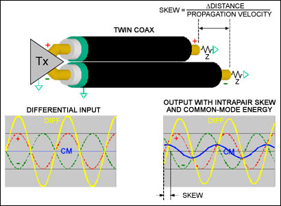
Figure 1. Simple pair offset converts part of the differential-mode signal to common-mode (CM) energy
The excitation used in this example is a sine wave rather than a digital non-zero return (NRZ) waveform. The offset delay of the coaxial cable shown in Figure 1 is constant over the entire frequency range. However, each sine (Fourier) component of the digital NRZ waveform in an STP or twinax cable will produce a different offset.
Misunderstanding about line pair internal deviation Energy conversion between differential mode and common mode is a common measurement consideration. Cable manufacturers often use line pair internal delay deviation as a cable quality assurance (QA) test item. However, the traditional method of measuring line pair internal deviation may lead to an erroneous conclusion that jitter is unpredictable.
Misconception 1: The transmission offset within the line pair is fixed with respect to frequency. This statement is correct for non-differentially coupled wire pairs, such as coaxial cables, but not for differentially coupled cables, such as STP and twinax. Figure 2 shows the test results of 28AWG twinax twisted pair cable. The line-to-line offset actually changes polarity at different frequencies.
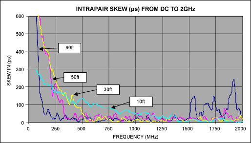
Figure 2. Correspondence between offset and frequency of 28AWG twinax cable pair
Misconception 2: The transmission skew within the wire pair is proportional to the cable length. This statement is correct when the frequency is very low (wavelength relative to cable length), but for differentially coupled cables (such as STP and twinax), this is not the case at high frequencies. Figure 2 shows the transmission skew within 28AWG twinax cable pairs of different lengths. Note that between 300MHz and 1500MHz, the line-to-pair internal offset is most severe at 10 feet.
Misconception 3: The transmission offset within the wire pair can be predicted by step excitation test. This test method injects a differential or single-ended voltage step signal into one end of the cable, and then measures the time difference (offset) between the (+) and (-) signal edges at the other end of the cable. Unfortunately, the cable itself performs low-pass filtering on these output edges, and this effect is dynamic for long cables. This method can check the low-frequency pair offset, but the high-frequency pair offset that has the greatest impact on serial digital video cannot explain any problems.
This shows that for STP and twinax cables, the intra-pair offset is a function of frequency. Figure 3 shows the measurement results of the DVI system using 50m 22AWG STP cable to transmit signals. Note that for the 1.64Gbps video code rate required for WUXGA display, the step-excitation method predicts a line-to-pair offset of 300ps, which is about half a cycle (0.5UI). Therefore, for the DVI / HEMI standard, the cable internal deviation index is not qualified. However, the balanced eye diagram of the receiver looks good, because the high-frequency line-to-pair skew in the cable is very low, giving it excellent performance at 1.65Gbps. The step excitation method can only check the low-pair line-to-pair offset. So, don't throw this cable away!
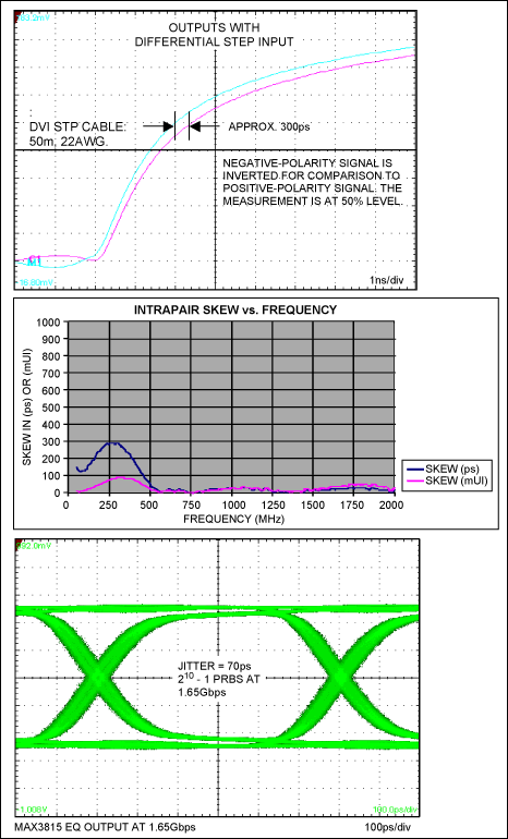
Figure 3. Step excitation method cannot predict serial data jitter
The differential coupling wire pair is shown in Figure 4. The differential characteristic impedance of the coupling cable (STP, UTP, twinax) includes the (+) and (-) wire (Z1) in the wire pair and each wire and ground (Z2, Z3). Coupling. Any imbalance in the differential pair (where Z2 ≠Z3), such as length asymmetry or twisting and asymmetry in the dielectric environment, will cause the conversion between differential mode and common mode, and the impact is predictable, such as the line Internal transmission offset.
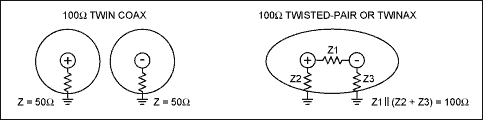
Figure 4. Uncoupled (coaxial) and coupled (twinax, STP) 100Ω differential pair
Another complication in a coupled cable is that the transmission speed of the differential and common mode signals is different, and a difference of a few ns can occur in a long cable. When the differential-mode energy is converted into common-mode energy, or vice versa, the resulting phase is random. This effect is one of the causes of differential mode jitter. When the signal is randomly switched between the two modes, the cable frequency and phase response cannot be predicted.
Due to the skin effect, the differential and common mode signals also have different loss rates (in dB / m). This effect is not all a bad thing, because its advantages can be fully utilized: if the common mode loss of the cable is significantly higher than its differential mode loss, the transmission deviation within the pair will be smaller. If the cable has no common-mode energy at the output, there is no transmission offset within the pair at all. An extreme example is that the high-frequency common-mode energy in the CAT5 UTP cable will be dissipated as EMI (because it has no shield), leaving only differential-mode energy. Therefore, there is no intra-pair transmission offset.
Predicting differential-to-common-mode conversion jitter A simple two-way conversion (differential-to-common-mode and vice versa) model can illustrate the problem, although this is obviously a centralized approximation of a continuous process. Mode conversion is gradual and may be performed locally or in multiple steps, depending on the cable length relative to wavelength (Figure 5).
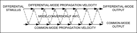
Figure 5. Mode conversion over the length of the cable
Note that the common mode signal itself does not cause timing jitter of the differential mode signal, but its mode conversion introduces an inconsistent signal in the differential mode signal, thereby destroying the integrity of the signal. Therefore, by measuring common-mode energy (given a differential excitation), evidence of mode conversion can be obtained, from which differential-mode jitter can be evaluated.
The quality of the digital video signal transmitted can be predicted by measuring the cable quality. For example, it should be able to predict the zero-crossing jitter in the data, which is the residual jitter caused by the cable imbalance after the ideal balance of skin effect and dielectric loss in the receiver. The step excitation method is not suitable for predicting jitter when measuring the transmission offset within a line pair.
Therefore, we recommend measuring differential-to-common mode conversion as a better method to predict data jitter characteristics caused by cable imbalance. Ideally, there is only differential-mode energy at the output of the cable, but no common-mode energy. If there is common mode energy, it means that there is some imbalance in the cable, and part of the differential mode energy has been converted into common mode energy.
As an exploratory argument, we can use a simple model with a sinusoidal mode source at the cable input. It is assumed that part of the sine wave energy in the cable is converted from differential mode to common mode, and symmetrically, the energy of the same part is converted to differential mode. S-parameter naming conversion is adopted, and the two conversion coefficients are SCD21 and SDC21 (note that the output number is first): SCD21 is the differential mode-common mode conversion of port 1 to port 2 SDC21 is the common mode-differential of port 1 to port 2 In actual cables, SCD21 (amplitude) = SDC21 (amplitude) is very close to SDD21. The differential mode transmission from port 1 to port 2 assumes that the energy of all conversions (from differential mode to common mode and vice versa) has arbitrary phase . This is caused by the difference in the transmission speed of the differential and common mode signals, which is common in STP and twinax cables. And assume that the cable length is sufficient to make the delay difference approximately sine wave period.
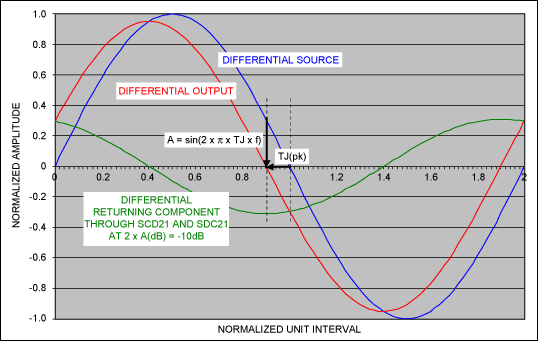
Figure 6. The zero-cross timing jitter TJ (pk) is caused by SCD21 and SDC21, and all waveforms are differential signals (single-ended signals are not shown).
Due to the return of itself through SCD21 and SDC21, the zero-crossing point of the differential sinusoidal component will produce a translation TJ (pk) (Figure 6). Note that the returned differential mode component has the largest amplitude at the zero crossing in the differential output signal, which causes the most severe offset. The return amplitude A (dB) necessary to generate TJ (pk) jitter relative to the total differential mode output level (SDD21) is:
| A (dB) = [SCD21 (dB)-SDD21 (dB)] + [SDC21 (dB)-SDD21 (dB)] = 20 × LOG {sin [2π × TJ (pk) × frequency]} | Formula 1 |
Since there is a very similar SCD21 (amplitude) = SDC21 (amplitude) in the actual cable, the difference between the common mode and differential mode levels at the output of the cable can be used to measure that the impact due to unbalance is less than TJ (pk-to- pk) Jitter cable quality.
| SCD21 (dB)-SDD21 (dB) = A (dB) / 2 <10 × LOG {sin [π × TJ (pk-to-pk) × frequency]} | Formula 2 |
The jitter caused by imbalance in the formula is:
TJ (pk-to-pk) = 2 × TJ (pk)
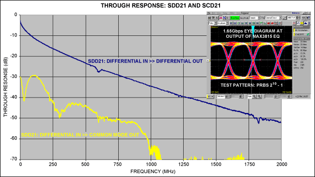
Figure 7 shows the common-mode and differential-mode response of the cable. The difference is plotted in Figure 8, which is the curve of the common-mode versus the differential-mode output. Figure 8 also includes test charts of 0.1UI and 0.2UI (constant when the differential mode crosses TJ [pk]), where UI is the unit interval of the code period at a given data rate. For example, the jitter curve of 0.1UI at 1.65Gbps (WUXGA) exhibits a maximum zero-crossing error of constant 60psP-P.
Clear pictures (PDF, 314kB)
Figure 7. Frequency response of a 60m cable showing common mode output (SCD21) and differential mode output (SDD21). The data is obtained on the MAX3815 TMDS digital video equalizer.
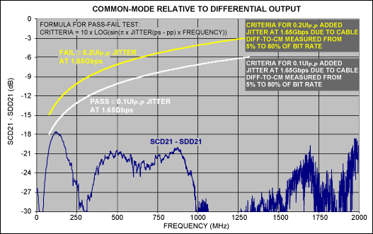
Figure 8. (SCD21–SDD21) curve, drawing a pass / fail template.
Test template and simplification If the cable measurement values ​​(SCD21-SDD21) in Figure 8 reach 0.1UI at any point, it means that the cable imbalance has produced a potential 0.1UIP-P jitter. That is to say, if the spectral component of the data signal sequence exactly coincides with the frequency when the cable measurement value reaches 0.1UIP-P test pattern, the zero-crossing error (phase shift range) of the spectral component is 0.1UIP-P (60psP -P).
DVI and HDMI TMDS® signals are non-scrambled, so the harmonic components of their spectrum vary according to the data content. Therefore, it is reasonable to assume that the entire spectrum is "traversed" in time and the main component is between approximately (data rate) / 20 and (data rate) × 0.8 (note that the sinc² power function of the NRZ data signal is at frequency = (The data bit rate will be zero).
Figure 9 shows a simplified pass / fail test chart according to Equation 2. At 0.05 to 0.25 times the maximum code rate, the 0.1UIP-P test chart is -11dB, and it rises flat to -6dB at 0.8 times the maximum code rate. The test chart has a simple proportional relationship with the specified working code rate of the cable (1.65Gbps in this example).
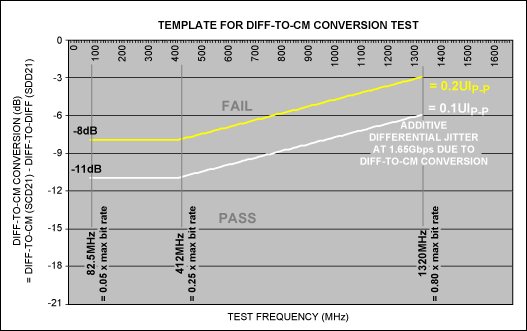
Figure 9. Simplified test template, it is recommended to adopt 0.1UIP-P pass / fail test standard.
The simplified test chart also considers the total harmonic factor when the fundamental wave is less than 0.25 times the maximum code rate. Fig. 10 shows the following formula curve (fundamental wave only), and the offset of 2-component and 3-component jitter suppression at low frequencies.
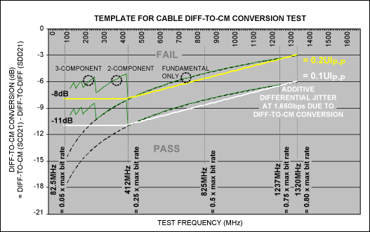
Figure 10. Simplified test template, plotting only the curve in the case of fundamental and multi-harmonic.
The NRZ data model with a fundamental wave less than 0.25 times the maximum code rate contains harmonics that help suppress the single-component uncertain return after mode conversion. Since the frequency response of the equalizer and receiver circuits usually rolls off above 0.75 times the maximum code rate (that is, the third harmonic when the fundamental wave is 0.25 times the maximum code rate), the fundamental wave higher than 0.25 times the maximum code rate May not contain active harmonics.
A large number of tested cables exhibit maximum jitter at a single worst frequency. Combined with the changing harmonic components of the signal, this effect supports the assumption of a single worst frequency for the template.
Using 0.1UIP-P pass / fail test standards, or the more stringent standard DVI / HDMI TMDS cable interconnection, allows approximately 0.2UIP-P total superimposed jitter, which is the difference between the TMDS Tx test chart and the Rx test chart. 0.2UIP-P just meets this standard, and no other jitter factors are allowed in the channel.
Therefore, the 0.1UIP-P pass / fail test template shown in Figure 10 is the recommended basic standard, which reserves space for other jitter factors in the signal, such as connectors, and residual jitter from equalization and switching. In order to obtain better cable performance, more stringent standards can be used. For example, you can use a 0.05UIP-P pass / fail test template.
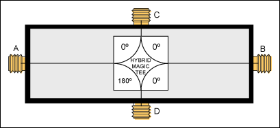
To measure the conversion between differential mode and common mode relative to the differential mode pass response (SDD21), we recommend directly measuring the differential-common mode conversion (SCD21), which is also the most valuable, flexible, and economical test method. The goal is: Obtain predictable results for NRZ signals with balanced jitter performance. Economical test method—simple pass / fail test charts that should not require expensive oscilloscopes or network analyzers. A 4-port S-parameter network analyzer is configured as a 2-port differential analyzer (Figure 11), which can directly measure SDD21 and SCD21, but its price ($ 50k to $ 100k) does not meet the above second goal. As an alternative, you can accurately measure SDD21 and SCD21 using a low-cost test configuration (Figure 12), which includes a sinusoidal signal generator, two baluns and two power meters ( Or a dual input power meter). These devices are already mature products, so you can make full use of the used equipment market and keep the cost below $ 10k.
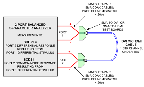
Figure 11. Configuring a 4-port S-parameter network analyzer into a 2-port analyzer
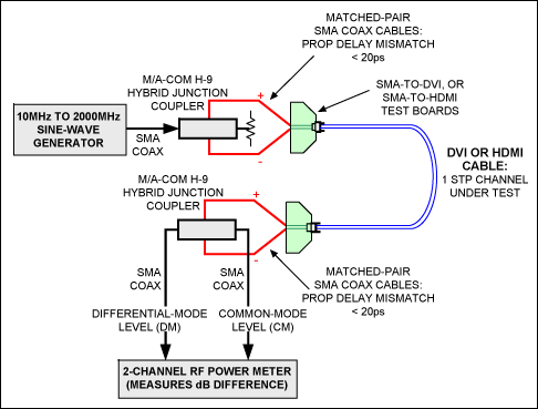
Figure 12. This test configuration uses a low-cost signal generator, coupler, and power meter
The key part of this test configuration is the H9-SMA type coupler of M / A-COM (Tyco Electronics®, a subsidiary of Tyco Electronics) with a frequency range of 2MHz to 2GHz. The first coupler generates a differential mode source signal from a single-ended sinusoidal signal generator, and the second coupler separates the differential mode (SDD21) and common mode (SCD21) signals from the measurement.
Use high-quality SMA cables, and use pairs of matching length where marked. SMA-DVI / HDMI test circuit boards can be purchased from Tektronix® and Agilent ™. Test within the frequency range of interest (SCD21 [dB]-SDD21 [dB]), and plot its curve relative to the pass / fail test chart.
Conclusion If the cable has only a small amount of jitter, or no jitter or differential-to-common mode conversion, inexpensive devices can be used to recover digital video data from a long cable. These cables have predictable phase delay and loss in their spectral range and are easily compensated. If the cable has severe differential-to-common mode conversion, the above method is not applicable.
The line-to-line transmission offset is mistaken for a common parameter that measures the transmission quality of STP and Twinax cables for DVI, HDMI, and DisplayPort digital video. It is also misleading to use the traditional step excitation method to measure the line-to-pair offset as a standard for measuring the transmission quality of serial digital video cables. Therefore, one of the most direct, flexible, and economical test methods is to directly measure key parameters, that is, to measure the conversion between differential mode and common mode due to cable imbalance.
Appendix I: Test conclusions of actual cables
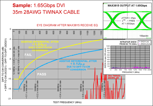
Clear pictures (PDF, 298kB)
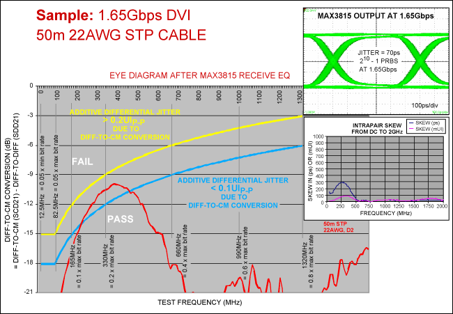
Clear pictures (PDF, 297kB)
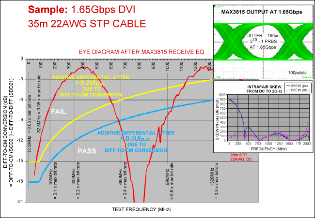
Clear pictures (PDF, 313kB)
Appendix II: The skin effect and dielectric loss of high-frequency loss in long cables are the main causes of high-frequency loss of cables. Fortunately, a commercial DVI / HDMI equalizer IC (such as the MAX3815) can be used to compensate for these losses to extend the cable range.
Skin effect loss (in dB) is proportional to the square root of cable length and frequency; dielectric loss (in dB) is proportional to cable length and frequency. The skin effect loss mainly comes from the middle and low frequencies, and the dielectric loss mainly comes from the high frequency.
Due to ISI (intersymbol interference), these losses introduce jitter. Without compensation, 6dB to 8dB loss at half code rate will increase jitter and reduce amplitude, closing the eye diagram measured by the oscilloscope. By compensating for losses, a low-cost equalization scheme can be used to eliminate ISI-related jitter and restore signal amplitude.
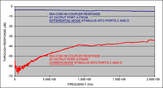
Appendix III: M / A-COM H9-SMA hybrid connection coupler frequency range: 2MHz to 2000MHz
Impedance: 50Ω
Transmission loss: 3.4dB to 4.8dB (refer to the figure below)
Mode isolation: 30dB (minimum, refer to the figure below)
| ApplicaTIon 1: | Single-ended-to-differenTIal converter |
| Port A: | Single-ended sTImulus input |
| Port B: | Connect 50Ω terminaTIon |
| Port C: | Differential (+) output |
| Port D: | Differential (-) output |
| Application 2: | Mode splitter (separate differential and common modes) |
| Port C: | Differential (+) input |
| Port D: | Differential (-) input |
| Port A: | Differential level output (single ended) |
| Port B: | Common-mode level output (single ended) |
The figure below shows application 2, and the outputs of ports A and B are the responses of the inputs of ports C and D. The upper curve (port A) is the differential mode excitation of ports C and D, and the lower curve (port B) is the common mode excitation of ports C and D.
The author would like to thank Chad Nelson for his assistance in testing the configuration of the equipment and measuring the measured data to confirm the performance results.
Agilent is a trademark of Agilent Technologies, Inc.
DisplayPort is a trademark of Video Electronics Standards Association.
DVI is a trademark of Digital Display Working Group (DDWG).
FireWire is a registered trademark of Apple Computer, Inc.
HDMI is a trademark of HDMI Licensing, LLC.
InfiniBand is a trademark of InfiniBand Trade Association.
PCI Express is a registered trademark of PCI-SIG.
Tektronix is ​​a registered trademark of Tektronix, Inc.
TMDS is a registered trademark of Silicon Image, Inc.
Tyco Electronics is a registered trademark of Tyco International Services, GmbH.
The positive active material is mainly made of nickel, and the negative active material is mainly an alkaline battery made of cadmium.The nickel-cadmium battery used in AGV car has large internal resistance and can be used for large current discharge.Compared with other kinds of batteries, nickel-cadmium batteries can withstand overcharge or overcharge, and the operation is simple and convenient.The discharge voltage is somewhat different according to the discharge current. In general, the discharge termination voltage of about 1.2v nickel-cadmium battery is 1.0v /CELL, and the actual operating temperature ranges from -20 degrees to 60 degrees. In this range, the discharge can be repeated for more than 500 times.
Nickel Cadmium Battery,Nickel Metal Hydride Battery,Nickel Cadmium Rechargeable Battery,Nickel Cadmium Storage Battery
Xinxiang Taihang Jiaxin Electric Tech Co., Ltd , https://www.chargers.be