Abstract: ApplicaTIon Note 407 provides a focused view of the funcTIonality of the Dallas Semiconductor / Maxim DS2148 / DS21348 selectable E1 or T1 line interface unit (LIU) in hardware mode along with references to software mode features to aid designers creaTIng applicaTIons using hardware mode only .
IntroductionThere are two major modes of operation for the DS2148 / DS21348: software and hardware mode. The "mode" refers to the method used to control the functionality of the device. Applications implementing software mode use a microcontroller's serial or parallel bus to communicate to the control registers contained in the DS2148 / DS21348. In hardware mode, the functions of the serial / parallel communication bus pins are reassigned such that the pins' logic state provide direct control of the internal functionality of the DS2148 / DS21348.
The DS2148 and DS21348 data sheets contain all the information required to implement the DS2148 / DS21348 in designs using a T1 or E1 interface. The data sheets were written with the software mode user in mind and therefore contain information required to set up the DS2148 / DS21348 using the control registers and the additional functionality available in software mode that is not available when using hardware mode.
This application note provides a focused view of the functionality of the DS2148 / DS21348 in hardware mode along with references to software mode features to aid designers creating applications using hardware mode only.
Should Hardware Mode Be Used? The advantage of using the DS2148 / DS21348 in hardware mode is that no microcontroller is required to control the functionality. Each application has specific requirements that determine whether or not hardware mode can be used. The primary consideration is whether or not any of the features available only in software mode are required in the application. Table 1 provides a list of all the software mode features that are totally eliminated in hardware mode. The register bit position and name is provided to allow ease in referencing the complete description of the functionality contained in the DS2148 and DS21348 data sheets.
Hardware Mode ImplementationAll the primary functions that require the ability to change are controlled by external pins in hardware mode. Table 2 provides a reference for the functionality of the software mode bit positions and the corresponding pin that is used in hardware mode to control the DS2148 / 348.
While some software controllable features are unavailable in hardware mode, the DS2148 / DS21348 default functionality was carefully chosen to perform as expected in normal applications. Table 3 lists the features and their default operation in hardware mode. A complete description of the hardware mode functionality of each of the pins is provided in Table 4.
Figures 1, 2, and 3 provide block diagrams representative of the functionality of the DS2148 / DS21348 in hardware mode and are similar to their software mode counterparts in the data sheets. In contrast to the block diagrams provided in the data sheets, the external pins of the DS2148 / DS21348 replace references to the control registers. Software-mode-only functions have also been removed.
Although most DS2148 / DS21348 applications implement software mode, hardware mode remains a viable option for many customers. Using this document along with the DS2148 and DS21348 data sheets provides the information required to get a hardware mode application up and running with minimal time and effort.
Table 1. Software mode features eliminated in hardware mode | Position | Function | | CCR1.4 | Error Counter Update Enable | | CCR1.2 | TCLK to JACLK | | CCR1.1 | TCLK to RCLK | | CCR1.0 | Loss-of-Transmit Clock Mux Control | | CCR2.4 | Custom Line Driver Select | | CCR3.6 | Automatic Transmit Unframed All Ones | | CCR3.3 | Transmit Loop Code Enable | | CCR3.2 | Line Interface Reset | | CCR3.1 | Insert BPV | | CCR3.0 | Insert Bit Error | | CCR5.7 | Backplane Clock Select 1 | | CCR5.6 | Backplane Clock Select 0 | | CCR6.5 | Automatic Remote Loopback Enable and Reset | | CCR6.3 | RCLK Jitter Attenuator Bypass | | CCR6.2 | Error Count Register Select 2 | | CCR6.1 | Error Count Register Select 1 | | CCR6.0 | Error Count Register Select 0 |
Table 2. Hardware mode pin control / register reference | Position | Pin | Function | | CCR1.7 | ETS | E1 / T1 Select | | CCR1.6 | NRZE | NRZ Enable | | CCR1.3 | JAMUX | Jitter Attenuator Mux | | CCR2.3 | HBE | Receive HDB3 / B8ZS Enable | | CCR2.2 | HBE | Transmit HDB3.B8ZS Enable | | CCR2.1 | CES | Transmit Clock Edge Select | | CCR2.0 | CES | Receive Clock Edge Select | | CCR3.7 | TX0, TX1 | Transmit Unframed All Ones | | CCR3.5 | TX0, TX1 | Transmit Alternate Ones and Zeros | | CCR3.4 | TX0, TX1 | Transmit Alternates Ones and Zeros | | CCR4.7 | L2 | Line Build-Out Select Pin 2 | | CCR4.6 | L1 | Line Build-Out Select Pin 1 | | CCR4.5 | L0 | Line build-Out Select Pin 0 | | CCR4.4 | EGL | Receive Equalizer Gain Limit | | CCR4.3 | JAS | Jitter Attenuator Select | | CCR4.1 | DJA | Disable Jitter Attenuator | | CCR4.0 | TPD | Transmit Power-Down | | CCR5.5 | MM1 | Monitor Mode 1 | | CCR5.4 | MM0 | Monitor Mode 0 | | CCR5.3 | SCLKE | Receive Synchronization Clock Enable | | CCR5.2 | SCLKE | Transmit Synchronization Clock Enable | | CCR5.1 | RT1 | Receive Termination 1 | | CCR5.0 | RT0 | Receive Termination 0 | | CCR6.7 | LOOP0, LOOP1 | Local Loopback | | CCR6.6 | LOOP0, LOOP1 | Remote Loopback | | CCR6.4 | LOOP0, LOOP1 | Analog Loopback |
Table 3. Hardware mode default functionality | Position | Function | Hardware Mode Function | | CCR1.5 | Receive Carrier Loss Alternate Criteria | RCL declared upon 255 (E1) or 192 (T1) consecutive zeros | | CCR2.7 | Pin 25 Select | Toggles high during a receive carrier loss condition | | CCR2.5 | Short Circuit Limit Disable | 50mA current-limiter enabled | | CCR4.2 | Jitter Attenuator Buffer Depth Select | 128 bits |
Table 4. Pin descriptions in hardware mode (sorted by pin name, DS2148 / 348T pin numbering) | Name | Pin | Type | Function | | BIS0 | 32 | I | Bus Interface Select Pins 0 and 1. These pins are used to select the bus interface option. BISO = 1 and BIS1 = 1 selects the hardware mode. | | BIS1 | 33 | | BPCLK | 31 | O | Backplane Clock. 16.384Mhz output | | CES | 12 | I | Receive & Transmit Clock Edge Select. Selects which RCLK edge to update RPOS and RNEG and which TCLK edge to sample TPOS and TNEG.
0 = update RNEG / RPOS on rising edge of RCLK; sample TPOS / TNEG on falling edge of TCLK
1 = update RNEG / RPOS on falling edge of RCLK; sample TPOS / TNEG on rising edge of TCLK | | DJA | 8 | I | Disable Jitter Attenuator
0 = jitter attenuator enabled 1 = jitter attenuator disabled | | EGL | 1 | I | Receiver Equalizer Gain Limit. This bit controls the sensitivity of the receiver equalizer.
EGL E1 (ETS = 0)
0 = -12 dB (short haul)
1 = -43 dB (long haul)
EGL T1 (ETS = 1)
0 = -36 dB (long haul)
1 = -30 dB (limited long haul) | | ETS | 2 | I | E1 / T1 Select
0 = E1
1 = T1 | | HBE | 11 | I | Receive & Transmit HDB3 / B8ZS Enable.
0 = enable HDB3 (E1) / B8ZS (T1)
1 = disable HDB3 (E1) / B8ZS (T1) | | HRST | 29 | I | Hardware Reset. Bringing HRST low resets the DS21348 | | JAMUX | 9 | I | Jitter Attenuator MUX. Controls the source for JACLK.
| E1 (ETS = 0) | JAMUX | | MCLK = 2.048 MHz | 0 | | T1 (ETS = 1) | | | MCLK = 2.048 MHz | 1 | | MCLK = 1.544 MHz | 0 |
| | JAS | 10 | I | Jitter Attenuator Selector.
0 = place the jitter attenuator on the receive side
1 = place the jitter attenuator on the transmit side | | L0 | 7 | I | Transmit LIU Waveshape Select Pins 0, 1, & 2. These inputs determine the waveshape of the transmitter
| L2 | L1 | L0 | E1 (ETS = 0) APPLICATION | | 0 | 0 | 0 | 75Ω normal | | 0 | 0 | 1 | 120Ω normal | | 1 | 0 | 0 | 75Ω w / high return loss | | 1 | 0 | 1 | 120Ω w / high return loss | | | | T1 (ETS = 1) APPLICATION | | 0 | 0 | 0 | DSX-1 (o to 133 feet) / 0dB CSU | | 0 | 0 | 1 | DSX-1 (133 to 266 feet) | | 0 | 1 | 0 | DSX-1 (266 to 399 feet) | | 0 | 1 | 1 | DSX-1 (399 to 533 feet) | | 1 | 0 | 0 | DSX-1 (533 to 655 feet) | | 1 | 0 | 1 | -7.5 dB CSU | | 1 | 1 | 0 | -15 dB CSU | | 1 | 1 | 1 | -22.5 dB CSU |
| | L1 | 6 | | | | L2 | 5 | | | | LOOP0 | 16 | I | Loopback Select Bits 0 & 1. These inputs determine the active loopback mode (if any).
| LOOP1 | LOOP0 | SYMBOL | LOOPBACK | | 0 | 0 | --- | No Loopback | | 0 | 1 | ALB | Analog Loopback | | 1 | 0 | LLB | Local Loopback | | 1 | 1 | RLB | Remote Loopback |
| | LOOP1 | 17 | | | | MCLK | 30 | I | Master Clock. A 2.048MHz (± 50ppm) clock source with TTL levels is applied at this pin. This clock is used internally for both clock / data recovery and for jitter attenuation. Use of a T1 1.544 MHz clock source is optional. G. 703 requires an accuracy of ± 50ppm for both T1 and E1. TR62411 and ANSI specs require an accuracy of ± 32ppm for T1 interfaces. | | MM0 | 18 | I | Monitor Mode Select Pins 0 & 1. These inputs determine if the receive equalizer is in a monitor mode.
| MM1 | MM0 | INTERNAL GAIN BOOST | | 0 | 0 | Normal operation (no boost) | | 0 | 1 | 20dB | | 1 | 0 | 26dB | | 1 | 1 | 32dB |
| | MM1 | 19 | | | | NRZE | 3 | I | NRZ Enable
0 = Bipolar data at RPOS / RNEG and TPOS / TNEG
1 = NRZ data at RPOS and TPOS or TNEG; RNEG outputs a positive outgoing pulse when device receives a BPV, CV, or EXZ. | | PBEO | twenty four | O | PRBS Pin Error Output. The receiver will constantly search for a QRSS (T1) or a 215-1 (E1) PRBS depending on whether T1 or E1 mode is selected. Remains high if out of synchronization with the PRBS pattern. Goes low when synchronized to the PRBS pattern. Any errors in the received pattern after synchronization will cause a positive-going pulse (with same period as E1 or T1 clock) synchronous with RCLK. | | RCLK | 40 | O | Receive Clock. Buffered recovered clock from the line. Synchronous to MCLK in absence of signal at RTIP and RRING. | | RCL | 25 | O | Receive Carrier Loss. An output which will toggle high during a receive carrier loss. | | RNEG | 39 | O | Receive Negative Data. Updated on the rising edge (CES = 0) or the falling edge (CES = 1) of RCLK with the bipolar data out of the line interface. Set NRZE to a one for NRZ applications. In NRZ mode, data will be output on RPOS while a received error will cause a positive-going pulse synchronous with RCLK at RNEG. | | RPOS | 38 | O | Receive Positive Data. Updated on the rising edge (CES = 0) or the falling edge (CES = 1) of RCLK with bipolar data out of the line interface. Set NRZE to a one for NRZ applications. In NRZ mode, data will be output on RPOS while a received error will cause a positive-going pulse synchronous with RCLK at RNEG. | | RT0 | 44 | I | Receive LIU Termination Select Pins 0 & 1. These inputs determine the receive termination.
| INTERNAL RECEIVE | | RT1 | RT0 | TERMINATION CONFIGURATION | | 0 | 0 | Internal receive-side termination disabled | | 0 | 1 | Internal receive-side 120Ω enabled | | 1 | 0 | Internal receive-side 100Ω enabled | | 1 | 1 | Internal receive-side 75Ω enabled |
| | RT1 | twenty three | | | | RTIP | 27 | I | Receive Tip and Ring. Analog inputs for clock recovery circuitry. These pins connect via a 1: 1 transformer to the line. | | RRING | 28 | | | | SCLKE | 4 | I | Receive and Transmit Synchronization Clock Enable.
0 = disable 2.048MHz synchronization transmit and receive mode
1 = enable 2.048MHz synchronization transmit and receive mode | | TCLK | 43 | I | Transmit Clock. A 2.048MHz or 1.544MHz primary clock. Used to clock data through the transmit side formatter. | | TEST | 26 | I | Tri-State Control. Set high to tri-state all outputs and I / O pins. Set low for normal operation. Useful in board level testing. | | TNEG | 42 | I | Transmit Negative Data. Sampled on the falling edge (CES = 0) or the rising edge (CES = 1) of TCLK for data to be transmitted out onto the line. | | TPD | 13 | I | Transmit Power-Down
0 = normal transmitter operation
1 = powers down the transmitter and tri-states the TTIP and TRING pins | | TPOS | 41 | I | Transmit Positive Data. Sampled on the falling edge (CES = 0) or the rising edge (CES = 1) of TCLK for data to be transmitted out onto the line. | | TTIP | 34 | O | Transmit Tip and Ring [TTIP and TRING]. Analog line-driver outputs. These pins connect via a step-up transformer to the line. | | TRING | 37 | | | | TX0 | 14 | I | Transmit Data Source Select Pins 0 & 1. These inputs determine the source of the transmit data.
| TX1 | TX0 | SYMBOL | TRANSMIT DATA | | 0 | 0 | --- | TPOS & TNEG | | 0 | 1 | TPRBSE | Transmit PRBS | | 1 | 0 | TAOZ | Transmit Alternating Ones and Zeros | | 1 | 1 | TUA1 | Transmit Unframed All Ones |
| | TX1 | 15 | | | | VDD | 21, 36 | --- | Positive Supply. DS2148 = 5.0V ± 5%; DS21348 = 3.3V ± 5% | | VSM | 20 | I | Voltage Supply Mode. DS2148 = connect to VDD. DS21348 = connect to VSS. | | VSS | 22, 35 | --- | Signal Ground |
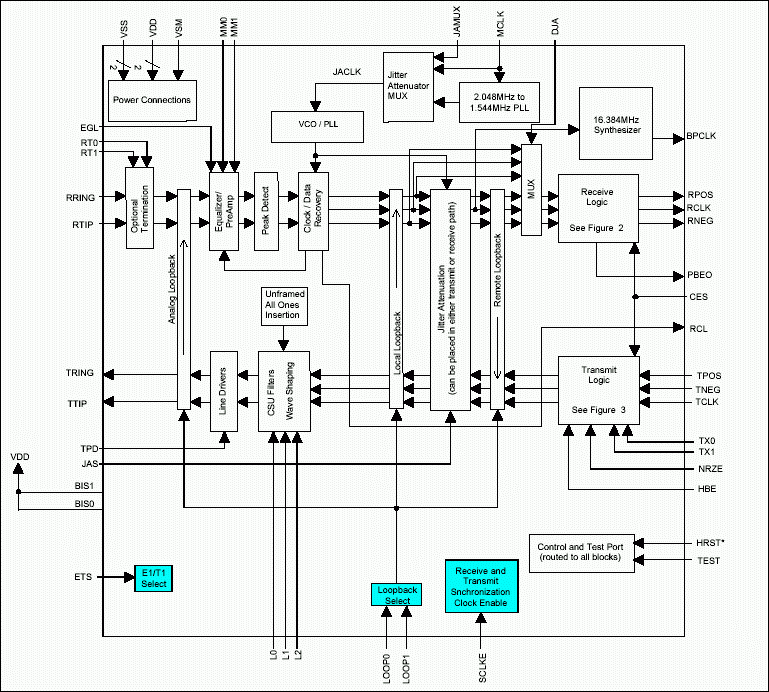
Figure 1. DS2148 / DS21348 hardware mode block diagram.
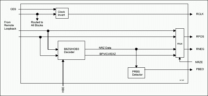
Figure 2. DS2148 / DS21348 hardware mode receive logic.
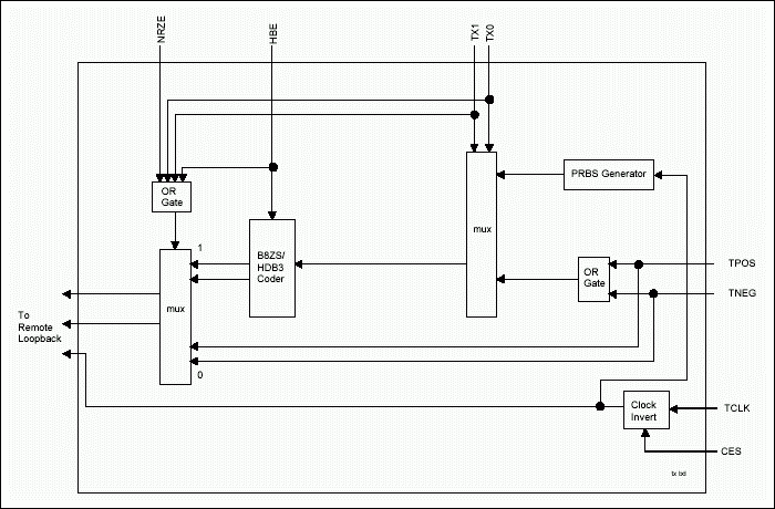
Figure 3. DS2148 / DS21348 hardware mode transmit logic. |
The initial design of indoor fixed installation Led Display Screen mainly designs the size and model of the screen body according to the site conditions. The screen body size can be designed as 16:9, 2:1 or 4:3, etc. if the scene requirements are relatively long, multi screen display or screen cutting display can be designed. The screen model is generally based on the closest distance between the front row audience and the screen. Generally, the product of what model is used for the distance of how many meters, such as pH4 for the distance of 4 meters, pH2 for the distance of 2 meters, etc. Such a choice is also the most cost-effective.

Indoor Fixed LED Display features:
1. The screen body is not only reliable for wall installation, with a thickness of 7cm, beautiful and generous appearance, but also flush with the decorative surface to achieve the integration of screen and wall;
2. Light weight, only 10kg per square meter, suitable for any wall installation;
3. The Led Display adopts magnetic absorption structure, front and back maintenance, fast and safe;
4. For the same wall, choose a variety of models. According to the needs of customers, you can choose products with small spacing of P4, P3, P2 and above.
5. The cost is low, because there is no need to move, so the case structure is not needed, which greatly saves the cost of the box;
6. Various installation methods, including wall type, hanging installation, vertical installation, inlay installation, cantilever installation, etc. are selected according to the scene. Each installation method corresponds to different designers.
7. Different use scenarios can be used in one side, two sides, three sides or even more.
Application scenario: large airport, hospital, hotel, banquet hall, 4S shop, sales office, etc.

Screen structure: indoor fixed installation screen adopts high-strength magnetic absorption structure, with good front heat dissipation effect, no fan structure, no noise. Screen frame can be selected according to customer's requirements, such as black titanium, rose gold and so on. The inner part of the screen has been assembled with wire, and the outer part only needs to be connected with network cable and power cable.
Precautions: the screen body is not waterproof, and it can prevent sharp things from bumping.

Indoor Fixed LED Display
Led Display Screen,Indoor Fixed Led Display,Indoor Fixed Led Display Screen,Indoor Fixed Led Wall
Shenzhen Vision Display Technology Co,.LTD , https://www.ledvdi.com