background
Data centers using FPGAs as accelerators have become mainstream, such as MS's Catapult, Amazon's Xilinx FPGA-based AWS F1, Intel's Altera, and Baidu. The data center has massive parallel data processing, high data throughput, low latency, and high energy efficiency. But there are two problems, the first is software problems, software migration and guarantees a certain accelerated workload; the second is hardware problems, equipped with many-core processors, 25-100G network interface cards, some DRAM/HBM Channel, easy timing closure, etc.
A GRVI Phalanx FPGA accelerator structure is now introduced. Among them, GRVI is an FPGA-based effective RISC-V computing unit, namely RISC-V RV321 soft processor core; Phalanx is a parallel FPGA accelerator framework, consisting of PE cluster, SRAM, accelerator, DRAM, I / O control Components, etc., reduce the cost and effort required to develop and manage FPGA accelerators; also need Hoplite NoC, which is an FPGA-based directional 2D ring-on-chip network system, using local memory sharing and Global information circulation, etc.

Fig. 1 GRVI operating unit
Let's take a look at GRVI Phalanx's 1680 core computing unit, which is based on a 32-bit RISCV microprocessor architecture. In a multi-core chip, unnecessary resources in each core are removed, with the goal of reducing The chip area of ​​each unit. Therefore, each GRVI processing unit is three-stage pipelined, adopting the RV321 core in user mode, and subtracting some unnecessary bits and other modules. The specific structure is shown in Fig. 1. Each GRVI operating unit requires 320 LUTs and can run at 375MHz. See the multi-core processor chip designed by blogger Jan Gray (see GRVI Phalanx: A Massively Parallel RISC-V FPGA Accelerator Framework for details): A 1680-core, 26 MB SRAM Parallel Processor Overlay on Xilinx UltraScale+ VU9Pâ€), characterized in that each GRVI operating unit is manually arranged, repeating 1680 times for a single processor unit in the UltraScale+ architecture of Xilinx FPGA. The generated file is downloaded to the Virtex UltraScale+VU9P FPGA chip on the board's Xilinx VCU118 Eval Kit.
Throwing a bunch of processor cores into Xilinx's Virtex UltraScale+ VU9P FPGA chip sounds interesting, but if you don't match every core with some memory, you can't give so many core processor cores Heavy duty. Therefore, each GRVI processor unit in the cluster will be equipped with 8 RISCV processor cores and 32 to 128 Kbytes of RAM, as well as additional accelerators. The entire acceleration chip consumes 31-40W, a single core consumes 24mW, the maximum throughput is 0.4TIPS, and the memory bandwidth can reach 2.5TB/s. The core clusters in the same chip are connected to each other, and the communication between the chip and the external I/O port is realized by HOPLITE routing to a NOC (on-chip network), and the data communication speed between the NOC nodes can reach 100 Gbps. HOPLITE routing is an FPGA-optimized directional routing designed specifically for 2D ring networks, as shown in Figure 2.
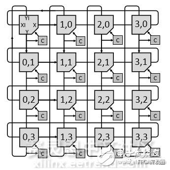
Fig. 2 A 400MHz 4*6*256 Hoplite NoC, 100 Gb/s links
The GRVI Phalanx cluster unit is shown in Figure 3. The software part requires a multi-threaded C++ compiler. The execution time of the information transfer is hierarchically arranged in the RV321MA GCC compiler of RISC-V, in order to be planned in the future. Support for some programming tools like OpenCL, P4 and others.

Fig. 3 GRVI Phalanx cluster
In other cases, the 80 core GRVI Phalanx was instantiated into the programmable Zynq Z-7020 SOC. This case was used as a teaching in the Digilent PYNQ-Z1 development board.
Even more surprising is the emergence of hardware development clouds that allow hardware designers to develop without having to buy expensive development boards. They only need to move their own mouse and keyboard through Amazon's platform: Amazon AWS EC2 F1.2XL and F1.16XL instances, you can find your own Verilog chip development code to create your own.
to sum up
The accelerator of the data center should be carried out simultaneously from software and hardware. The software needs to have an acceleration algorithm, and the portability and stability of the algorithm need to be considered. The hardware can use the solution of the multi-core processor analyzed in the text. Of course, software migration should be considered. Sex, the ease of use of the compiler tools, the design difficulties of the hardware itself, and the performance, power consumption, and ease of maintenance of the hardware. Xilinx FPGAs play an important role in parallel computing in data centers.
10 segment led bar ,red led bar ,yellow green led bar
Wuxi Ark Technology Electronic Co.,Ltd. , https://www.arkledcn.com