1 Introduction
A light emitting diode (LED) is a semiconductor device that converts electrical energy into a light solid state. Compared with traditional incandescent lamps, LEDs have the advantages of long service life, wide color gamut, durability, flexible design, simple control and environmental protection. Therefore, LED is considered to be the most promising light source in the future. Since red, green, and blue (RGB) tri-color LEDs can be mixed to get a very wide color gamut white light source, it makes it very attractive for liquid crystal display (LCD) backlighting applications, because it means that humans will have thinner, more An environmentally friendly liquid crystal display with a longer life, a higher dimming ratio, and a brighter color. Therefore, research articles on direct-lit LED backlights and light-guiding LED backlights have been published. The world's first LCD TV with RGB-LED hybrid backlighting was also available at Sony, which offers a very wide range of color reproduction and is 105% of the National Color System Committee's (NTSC) standard color gamut coverage. However, the problem of heat dissipation behind these research results still exists. The heat generated by the LED illumination process causes the output light intensity of the LED to decrease and the dominant wavelength to drift. These two factors can cause the color temperature of the display to change, resulting in different NTSC results. Furthermore, heat will also shorten the life of the display. Therefore, in order to ensure image quality and display reliability, heat dissipation research of backlight systems is crucial.
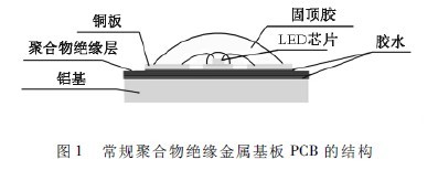
In order to improve the heat dissipation performance of the RGB-LED backlight system, two aspects can be considered: (1) Improve the heat dissipation performance of a single LED. (2) Improve the heat dissipation performance of the LED array. As an RGBLED backlight system designer, we chose the second option to solve the heat dissipation problem. In order to improve the heat dissipation performance of the LED array system, there are also two methods of heat dissipation: (1) Use a fan to increase the flow rate of air around the backlight system. (2) Reduce the thermal resistance from the junction to the environment. It is a better solution to design a printed circuit board with a light-emitting substrate with an economical design and excellent heat dissipation performance. The conventional polymer insulated metal substrate (IMS) technology, which is currently widely used, uses a polymer or epoxy material as an insulating layer, and its structure is shown in Fig. 1. This technique requires special treatment of the surface of the metal substrate, and the insulating layer The minimum thickness is approximately 75 microns, which will increase the thermal resistance of the entire insulated metal substrate. In addition, traditional IMS technology creates insulation and metal substrate delamination at high temperatures.
In this paper, we have implemented a new type of insulated metal substrate PCB using magnetron sputtering technology. We chemically form an insulating layer with a thickness of 30 to 35 microns on the surface of the aluminum substrate, and use magnetron sputtering to form the designed circuit on the insulating layer. This insulated metal substrate PCB has excellent heat dissipation properties and can eliminate delamination or peeling at high temperatures. The thermal resistance of the new insulating aluminum substrate and the conventional polymer insulated aluminum substrate were 4.78 ° C /W and 7.61 ° C / W, respectively.
2 Magnetron sputtering technology
2. 1 Basic sputtering process
Sputtering is a vacuum process that deposits materials such as metals, ceramics, and plastics onto a surface to form a thin film. The basic sputtering process is as follows: The electrons strike an inert gas atom (usually argon), making it an ion. These energetic ions bombard the target material to be deposited under the action of an electric field. The strong bombardment causes the target atoms to escape from the surface of the material, and finally forms an atomic layer film on the surface of the substrate under the action of the electric field. The thickness of the atomic layer film depends on the sputtering time.

2. 2 magnetron sputtering process
Figure 2 shows the whole process of magnetron sputtering. Compared with the basic sputtering process, the main difference between the two is that the magnetron sputtering process has a stronger magnetic field in the target region than the basic DC sputtering process. The magnetic field lines move in the target area and are not attracted to the substrate. Therefore, the magnetron sputtering process has three advantages over the basic sputtering process: (1) The plasma region is limited to the vicinity of the target material and does not impair the film being formed. (2) The distance of the electron motion becomes longer, increasing the probability of electron ionization of the argon atoms, which means that more target atoms will be bombarded, thereby increasing the efficiency of the sputtering process. (3) Magnetron sputtering produces the smallest amount of film impurities, which ensures the quality of the film.
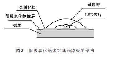
3 Anodized Insulating Aluminum-based Circuit Board Design
As shown in Figure 3, the anodized insulating aluminum-based circuit board consists of three layers: an aluminum base layer, an anodized insulating layer and a metallized layer, wherein the metallized layer is composed of three layers of a base film, a conductive film and a solder film. .
3. 1 aluminum base layer
The aluminum base layer is the basis of this circuit board. The two factors should be considered in the selection of materials: (1) The selected aluminum material needs certain mechanical strength and processing performance; (2) It is suitable for oxidation and insulation treatment. Under certain conditions, the aluminum base layer can be processed into a fin shape.
3. 2 anodized insulation
The anodized insulating layer is formed into a microporous structure by a special anodizing treatment, and these microporous structures determine its electrical insulating properties. According to different processing technologies, its electrical strength reaches 250V to 3000V. The lines are drawn on this layer by photolithographic masking techniques. This design enables seamless splicing of the base layer and the insulating layer. At the same time, the LED chip will be directly connected to the layer, which makes the chip, printed circuit board and heat sink form a unified whole, which significantly improves the heat dissipation performance of the circuit board.
3. 3 metallization layer
The metallization layer is composed of a base film, a conductive film, and a solder film. The metallization layer not only satisfies the conductive function but also ensures a sufficient bonding force between the metallization layer and the anodized insulating layer. The circuit will be formed on this layer by magnetron sputtering, as shown in Figure 4.

1) Basement membrane
The thickness of the base film is between 0.1 and 0.15 μm, and the film is formed by depositing chromium or titanium metal using a magnetron sputtering technique. The role of the base film is mainly to provide a sufficient bonding force between the metallization layer and the anodized insulating layer. Using magnetron sputtering technology, this bonding force can reach 1000 N / cm2, making the connection between the two layers more stable and stable. In addition, the base film also has a very good high-temperature thermal resistance property, which ensures no foaming and peeling when the temperature is higher than 320 ° C / 10 s. Therefore, it is fully applicable to lead-free soldering technology.
2) Conductive film
The thickness of the conductive film is between 1 and 2 μm, and the film is formed by depositing copper using a magnetron sputtering technique, nickel or a copper-nickel alloy. The main functions of the conductive film mainly include two aspects, one is to carry a certain current density, and the other is to ensure the entire metallization through the buffering action of the conductive film when the base film and the solder film are deformed due to different expansion coefficients. Layer stability.
3) Welding film
The thickness of the solder film is between 0.3 and 0.8 μm, and the film is formed by depositing a metal having good thermal conductivity and solderability similar to gold and silver by magnetron sputtering. The main function of the solder film is to facilitate the soldering of electronic components including LEDs.
4 Manufacturing Process Technology
As shown in Figure 5, the entire process involves 5 steps, which we reduced to 3 parts.
